





Passive Components Blog
No Result
View All Result
  • Home
  • News
    • All
    • Aerospace & Defence
    • Antenna
    • Applications
    • Automotive
    • Capacitors
    • Circuit Protection Devices
    • electro-mechanical news
    • Filters
    • Fuses
    • Inductors
    • Industrial
    • Integrated Passives
    • inter-connect news
    • Market & Supply Chain
    • Market Insights
    • Medical
    • Modelling and Simulation
    • New Materials & Supply
    • New Technologies
    • Non-linear Passives
    • Optoelectronics and Isolation
    • Oscillators
    • Passive Sensors News
    • Resistors
    • RF & Microwave
    • Telecommunication
    • Weekly Digest
    YAGEO Nexensos M422 Pb-free platinum RTD graphic showing the operating temperature range, nominal resistance options and joining methods.

    YAGEO Introduces Pb-Free Platinum RTD Temperature Sensor

    Reference tantalum capacitor anode characterization, tantalum anode modeling, process selection and life-test verification.

    Tantalum Anode Design Combines Structural Benchmarks and Modeling

    Wk 45 Electronics Supply Chain Digest

    SCHURTER TCS6F IP67 sealed SMD tactile switch with white silicone actuator on dark background

    SCHURTER Unveils IP67 Tactile Switch in 6.2 × 6.2 mm Package

    YAGEO SMD 0603 ST Pt1000 chip sensor shown in front of rooftop HVAC equipment

    YAGEO SMD 0603 ST Pt1000 Sensor with Standard SMD Termination

    Power line EMI filter on a copper ground-plane fixture connected to a vector network analyzer with a toroidal balun

    How to Measure Filter Performance: Insertion Loss, VNA Fixtures and CM/DM Separation

    Assorted EMI and RF filter components: common mode choke, ferrite beads, feedthrough filter, X2 capacitor, cavity filter, ceramic coaxial resonators, thin-film filter and SAW/BAW packages

    Passive Filter Technologies Compared: LC, Ferrite, Feedthrough, Ceramic, Cavity, Microstrip, SAW and BAW

    Illustration of a thin-film capacitor stack with TiN electrodes and an ultrathin hafnium zirconium oxide ferroelectric layer on silicon

    Sub-Volt Ferroelectric HZO Capacitor Pairs Speed and Endurance

    Cut-open lithium-ion capacitor pouch cell showing stacked carbon electrodes and separators, with vials of carbon powder

    Lithium-Ion Capacitor Review Backs Hard Carbon//AC Pairing

    Trending Tags

    • Ripple Current
    • RF
    • Leakage Current
    • Tantalum vs Ceramic
    • Snubber
    • Low ESR
    • Feedthrough
    • Derating
    • Dielectric Constant
    • New Products
    • Market Reports
  • Knowledge Blog
  • Dossiers
    • Aerospace and Defense Passive Components Dossier
    • AI Hardware Dossier
    • Automotive Dossier
    • Industrial Robotics Dossier
    • Power Converter Dossier
    • Capacitor Dossier
    • Circuit Protection Dossier
    • Inductor Dossier
    • Resistor Dossier
    • Silicon Capacitors and Integrated Passives Dossier
  • Suppliers
    • Who is Who
  • PCNS
    • PCNS 2025
    • PCNS 2023
    • PCNS 2021
    • PCNS 2019
    • PCNS 2017
  • Events
  • Home
  • News
    • All
    • Aerospace & Defence
    • Antenna
    • Applications
    • Automotive
    • Capacitors
    • Circuit Protection Devices
    • electro-mechanical news
    • Filters
    • Fuses
    • Inductors
    • Industrial
    • Integrated Passives
    • inter-connect news
    • Market & Supply Chain
    • Market Insights
    • Medical
    • Modelling and Simulation
    • New Materials & Supply
    • New Technologies
    • Non-linear Passives
    • Optoelectronics and Isolation
    • Oscillators
    • Passive Sensors News
    • Resistors
    • RF & Microwave
    • Telecommunication
    • Weekly Digest
    YAGEO Nexensos M422 Pb-free platinum RTD graphic showing the operating temperature range, nominal resistance options and joining methods.

    YAGEO Introduces Pb-Free Platinum RTD Temperature Sensor

    Reference tantalum capacitor anode characterization, tantalum anode modeling, process selection and life-test verification.

    Tantalum Anode Design Combines Structural Benchmarks and Modeling

    Wk 45 Electronics Supply Chain Digest

    SCHURTER TCS6F IP67 sealed SMD tactile switch with white silicone actuator on dark background

    SCHURTER Unveils IP67 Tactile Switch in 6.2 × 6.2 mm Package

    YAGEO SMD 0603 ST Pt1000 chip sensor shown in front of rooftop HVAC equipment

    YAGEO SMD 0603 ST Pt1000 Sensor with Standard SMD Termination

    Power line EMI filter on a copper ground-plane fixture connected to a vector network analyzer with a toroidal balun

    How to Measure Filter Performance: Insertion Loss, VNA Fixtures and CM/DM Separation

    Assorted EMI and RF filter components: common mode choke, ferrite beads, feedthrough filter, X2 capacitor, cavity filter, ceramic coaxial resonators, thin-film filter and SAW/BAW packages

    Passive Filter Technologies Compared: LC, Ferrite, Feedthrough, Ceramic, Cavity, Microstrip, SAW and BAW

    Illustration of a thin-film capacitor stack with TiN electrodes and an ultrathin hafnium zirconium oxide ferroelectric layer on silicon

    Sub-Volt Ferroelectric HZO Capacitor Pairs Speed and Endurance

    Cut-open lithium-ion capacitor pouch cell showing stacked carbon electrodes and separators, with vials of carbon powder

    Lithium-Ion Capacitor Review Backs Hard Carbon//AC Pairing

    Trending Tags

    • Ripple Current
    • RF
    • Leakage Current
    • Tantalum vs Ceramic
    • Snubber
    • Low ESR
    • Feedthrough
    • Derating
    • Dielectric Constant
    • New Products
    • Market Reports
  • Knowledge Blog
  • Dossiers
    • Aerospace and Defense Passive Components Dossier
    • AI Hardware Dossier
    • Automotive Dossier
    • Industrial Robotics Dossier
    • Power Converter Dossier
    • Capacitor Dossier
    • Circuit Protection Dossier
    • Inductor Dossier
    • Resistor Dossier
    • Silicon Capacitors and Integrated Passives Dossier
  • Suppliers
    • Who is Who
  • PCNS
    • PCNS 2025
    • PCNS 2023
    • PCNS 2021
    • PCNS 2019
    • PCNS 2017
  • Events
No Result
View All Result
Passive Components Blog
No Result
View All Result

Connector Contact Design: Force, Wipe and PCB Alignment

18.10.2026
Reading Time: 6 mins read
A A
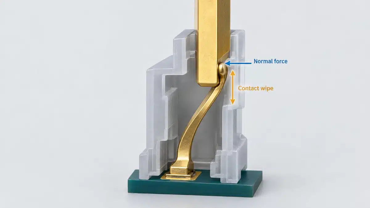
Conceptual Samtec connector contact illustration showing a deflected spring beam and sliding mating surfaces.

A connector’s electrical interface depends on a sequence of mechanical events: alignment, contact deflection and sliding engagement.

This contact-design guidance explains how spring geometry, normal force, contact wipe and plating work together—and why PCB spacing and dimensional tolerances belong in connector selection.

RelatedPosts

Samtec AcceleRate mP 10 mm Signal and Power Connectors

Samtec Links Automotive Connector Demands to Software-Defined Cars

Samtec 100-CM 1.0 mm RF Connectors Extend to 120 GHz

Key features and benefits

  • Contact deflection generates the force that presses mating surfaces together.
  • Contact geometry and spring material govern how the contact responds during mating.
  • Sliding engagement provides a cleaning action at the contact interface.
  • Plating works with contact geometry and normal force to establish the electrical connection.
  • Controlled board spacing and alignment help maintain the intended engagement across manufacturing tolerances.

These characteristics form an interconnected system. Selecting a plating finish independently of contact geometry, or choosing board spacing independently of mating depth, overlooks the mechanical conditions that create the electrical interface.

Technical highlights

Contact deflection creates normal force

During mating, at least one contact normally deflects. The contact’s geometry and material determine its response to this movement.

That deflection generates normal force: the force pressing the mating surfaces together. Insufficient force can produce an unreliable connection, but increasing force without regard to geometry is not a complete solution. The contact must generate the required force while remaining within its intended mechanical limits.

The spring material therefore has two roles. It must provide the mechanical behaviour required for repeatable deflection and the conductivity required for the electrical path. The relationship between these functions is central to connector structure and contact-spring design.

Contact wipe establishes the interface

Contact wipe is the sliding movement between mating contact surfaces as the connector engages. This movement helps remove contamination and surface films from the mating area.

Particles from surrounding processes, dust, oils and oxide films can interfere with electrical contact. Tin-plated surfaces can develop oxide films through exposure to air or humidity, making the cleaning action relevant to interface performance.

Available wipe depends on contact geometry, insertion depth and mechanical tolerances. A nominally mated connector must therefore retain sufficient engagement across the permitted dimensional range, not merely at the nominal assembly position.

Plating and geometry must work together

Connector contacts commonly use copper-alloy spring materials with a plated mating surface. Gold and tin have different interface characteristics and must be considered alongside normal force and wipe.

Gold resists oxidation and requires less normal force than tin. This relationship matters in low-profile, fine-pitch connectors, where contact geometry constrains the available spring movement and force.

The contact finish is consequently part of the mechanical design, not an independent purchasing option. Its interaction with the spring and mating surface is a central consideration in connector materials and processes.

Design factorFunctionSelection consideration
Contact geometryControls deflectionMechanical operating limits
Normal forcePresses surfaces togetherSpring behaviour and finish
Contact wipeCleans mating interfaceEngagement throughout tolerances
PlatingForms contact surfaceForce and wipe requirements
Board spacingSets mating depthPermitted insertion range
AlignmentPositions mating contactsCombined assembly tolerances

Application fit

Board-to-board connections

In a board-to-board assembly, stack height—the distance between the connected PCBs—affects contact engagement. Board spacing must remain within the connector’s permitted insertion range so the mating contacts retain the intended wipe.

Connector selection and mechanical stack design should therefore proceed together. Fixing PCB separation before considering mating depth can constrain the contact interface.

Low-profile and high-density assemblies

Reducing connector height creates a trade-off between package size and the mating length available for contact wipe. The contact still needs enough sliding engagement to perform its cleaning action.

Gold-plated interfaces can support contact systems with lower normal force than tin-plated interfaces. Plating choice must nevertheless remain tied to the selected contact geometry and its mating conditions.

Assemblies exposed to vibration and shock

Contact wipe and contact-point redundancy are relevant to connections that must withstand vibration and shock. The contact system must establish the intended interface during mating before it can maintain that interface in service.

Multiple connectors between the same PCBs

Using several connector pairs between two boards introduces interacting dimensional tolerances. Connector dimensions and placement on each PCB contribute to the final alignment.

Contact systems can accommodate some movement, but their deflection and wipe capabilities are finite. Tolerance stack-up analysis should establish whether every connector pair can engage within its intended mechanical range.

Design-in notes for engineers

  • Establish PCB stack height together with the mating connector pair, rather than treating board spacing as a separate decision.
  • Check minimum and maximum insertion depth against the assembled mechanical stack.
  • Evaluate contact wipe across dimensional tolerances, including connector placement on the PCB.
  • Assess plating, normal force and contact geometry together.
  • For multiple connector pairs, analyse combined alignment tolerances rather than each pair in isolation.
  • Include the expected contamination, vibration and shock conditions in contact-system selection.
  • Validate the final assembly under its actual operating conditions before production release.

Contact resistance is an electrical measurement, but the interface behind it is created mechanically. Alignment, spring deflection, normal force and wipe must work together to establish the intended connection.

Further reading

  • Connector Design/Selection/Assembly
  • How Much Gold is Needed for Connector Plating
  • Feedback from Connector Failure Analysis

Source

This article is based on the Samtec technical article and official connector-design documentation. Engineers should refer to the current manufacturer datasheet for final design and qualification.

References

  1. Making Contact: The Mechanical Life of a Connector, Part 1
  2. Is Contact Wipe Important?

Related

Recent Posts

Würth Elektronik ICS PowerBusbar PF vertical PCB busbars with flat metal bodies and press-fit pins.

Würth PowerBusbar PF: Vertical Press-Fit Busbars for PCBs

4.11.2026
36

Heatsink Design and Thermal Interface Materials for Reliable Electronics

27.4.2026
472

Coaxial Connectors and How to Connect with PCB

17.12.2025
1.6k

PCB Manufacturing, Test Methods, Quality and Reliability

18.6.2026
737

Circular Connectors Coding

26.11.2025
328
Image credit: Samtec

How to Match the Right Connector with Protocol Requirements

6.11.2025
93

Connector PCB Design Challenges

3.10.2025
156
source: Samtec

Best Practices for Cable Management in High-Speed and High-Density Systems

4.9.2025
278

What Track Width To Use When Routing PCB

6.6.2025
226

Upcoming Events

Nov 24
16:00 - 17:00 CET

Select the Correct Components for Your DC/DC Converter

Dec 1
16:00 - 17:00 CET

Developing low-noise mixed-signal systems

Dec 8
16:00 - 17:00 CET

WE-CCMF: Design Principles, Layout Guidelines and Measurement Results for High-Speed EMI Filtering

View Calendar

Popular Posts

  • Buck Converter Design and Calculation

    0 shares
    Share 0 Tweet 0
  • September 2026 Interconnect, Passives and Electromechanical Components Market Insights

    0 shares
    Share 0 Tweet 0
  • Boost Converter Design and Calculation

    0 shares
    Share 0 Tweet 0
  • Capacitor Charging and Discharging

    0 shares
    Share 0 Tweet 0
  • LLC Resonant Converter Design and Calculation

    0 shares
    Share 0 Tweet 0
  • RF Connector Types: How To Choose the Right One

    0 shares
    Share 0 Tweet 0
  • Passive Low Pass Filters: Fundamentals and EMI Design

    0 shares
    Share 0 Tweet 0
  • Flyback Converter Design and Calculation

    0 shares
    Share 0 Tweet 0
  • MLCC and Ceramic Capacitors

    0 shares
    Share 0 Tweet 0
  • Audio Capacitors: Choosing Capacitors for Crossover Circuits

    0 shares
    Share 0 Tweet 0

Newsletter Subscription


Passive Components Blog

© 2015–2026
All rights reserved

  • Home
  • Privacy Policy
  • EPCI Membership & Advertisement
  • About

No Result
View All Result
  • Home
  • Knowledge Blog
  • Dossiers
  • PCNS

© 2015–2026
All rights reserved