

MLCC and ceramic capacitors combine compact construction with a wide range of capacitance, voltage and high-frequency characteristics, but their suitability depends strongly on the dielectric and mechanical design. Class 1 ceramics provide stable, low-loss capacitance, while Class 2 ceramics provide higher capacitance density with greater dependence on voltage, temperature and time.
This guide explains construction, manufacturing, electrical behaviour, failure mechanisms and selection for design engineers and component engineers working on signal, RF, power-conversion and EMI-filtering applications.
Key Takeaways
- MLCC means multilayer ceramic capacitor: alternating internal electrodes connect multiple dielectric layers in parallel. Single-layer ceramic capacitors use one active dielectric layer and remain useful in RF, microwave, high-voltage and feedthrough applications.
- Class 1 dielectrics such as C0G, also commonly called NP0, suit stable filters, matching networks, timing and resonant circuits. Class 2 dielectrics such as X5R and X7R provide higher capacitance density, but nominal capacitance alone does not describe their in-circuit performance.
- For Class 2 MLCCs, evaluate capacitance at the actual DC bias, AC excitation, temperature and elapsed time. A temperature-characteristic code does not specify the DC-bias loss or guarantee interchangeability between suppliers.
- Low equivalent series resistance and inductance support decoupling and high-frequency operation, but capacitor placement, PCB connections, ripple-current heating and network resonances remain part of the design.
- Ceramic bodies are brittle. Board bending, thermal shock and unsuitable assembly processes can initiate cracks that later cause leakage or short circuits. Flexible terminations reduce transferred stress but do not make every failure mode fail-open.
- Select the exact part number and qualification for the application. Automotive qualification, high-reliability screening and safety approval address different requirements; a high DC voltage rating alone does not establish suitability for a mains-connected X or Y capacitor position.
Introduction to MLCC and Ceramic Capacitors
Ceramic capacitors use an insulating ceramic between conductive electrodes to store electric charge. Their behaviour depends on both the ceramic material and the physical arrangement of the electrodes, so construction and dielectric class must be considered separately. An introduction to the underlying quantities is available in the explanation of capacitance and capacitor operation.
The main construction families discussed here are single-layer ceramic capacitors, abbreviated SLC or SLCC, and multilayer ceramic capacitors, abbreviated MLCC. Both families include specialised products; neither construction, by itself, determines the temperature coefficient, voltage dependence, loss or qualification level. [1,2]
Single-layer ceramic capacitors
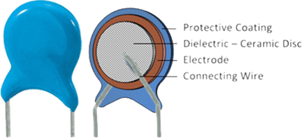
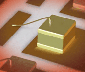
An SLCC has one active ceramic dielectric layer between its electrodes. The format may be an unencapsulated chip, a leaded disc, a tube or a specialised geometry. A simple layer arrangement can be useful where electrode access, RF behaviour, voltage spacing or physical integration matters more than achieving maximum capacitance in minimum volume.
- Simple active-layer construction, with capacitance determined by dielectric permittivity, electrode area and ceramic thickness.
- Available as economical general-purpose components and as specialised RF, microwave or high-voltage components; a single-layer construction is not inherently a low-cost product.
- Generally less scope for increasing capacitance through layer multiplication than an MLCC of comparable external dimensions.
- Loss and high-frequency performance depend on the dielectric, electrodes, connections and package. SLCCs should not be assigned universally higher ESR than MLCCs.
Multilayer ceramic capacitors
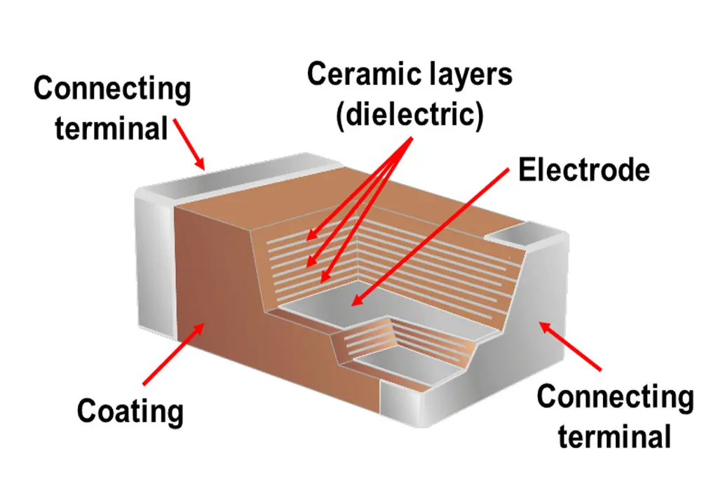
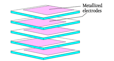
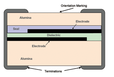
An MLCC contains alternating ceramic dielectric layers and internal metal electrodes. Successive electrode groups connect to opposite external terminations, placing the active dielectric gaps electrically in parallel. Increasing the number of active gaps increases capacitance without requiring a corresponding increase in PCB footprint. [2]
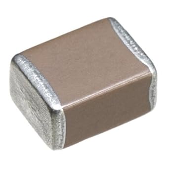
MLCC technology supports high-volume assembly, small packages, low ESR and a wide choice of electrode arrangements. These attributes make it useful for decoupling and filtering, while stable dielectric variants serve precision and RF functions. The available capacitance must nevertheless be evaluated together with its operating conditions rather than inferred from package size alone. [1,3]
Package sizes and miniaturisation
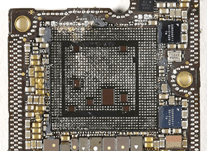
Rectangular chip capacitors are commonly described using either inch-based or metric size codes. Always state which system is being used: the same four digits can identify different dimensions in different systems. A size code describes nominal length and width, not the complete dimensional tolerance, component height, termination geometry or recommended PCB land pattern.
For example, the familiar inch-based 0805 package corresponds approximately to a 2.0 mm × 1.25 mm body and is commonly identified as metric 2012. Inch-based 0201 corresponds approximately to 0.6 mm × 0.3 mm, commonly identified as metric 0603. These are nominal package descriptions; the controlled drawing for the exact part determines the permissible dimensions.
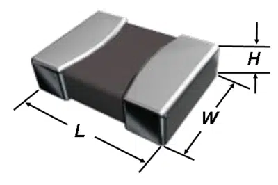
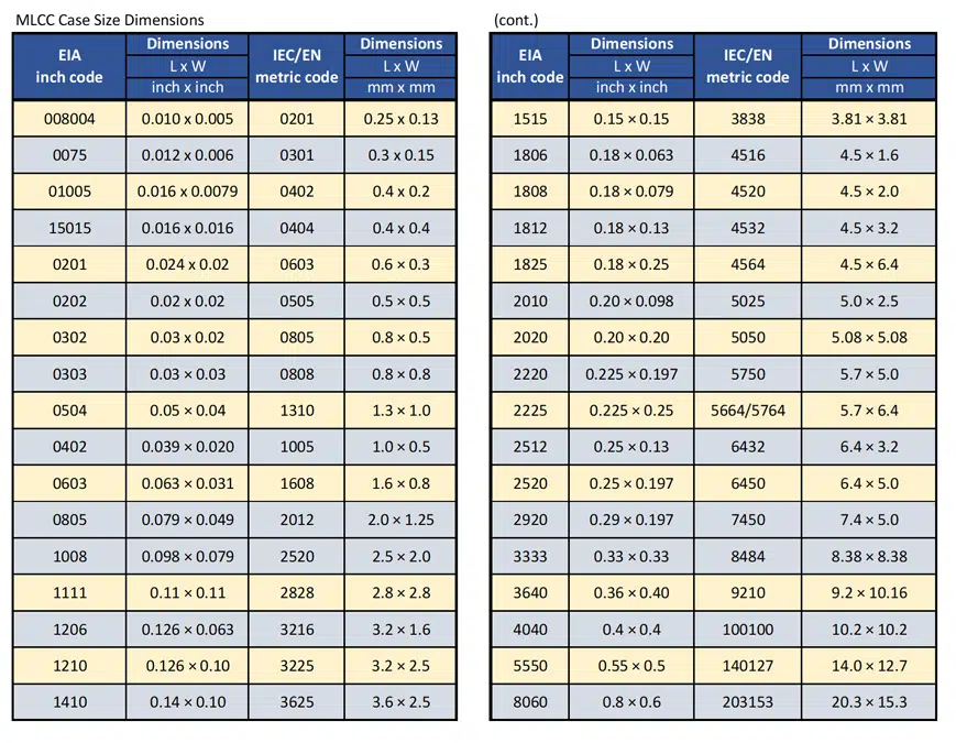
The article on MLCC case-size conventions explains the naming systems in more detail. Package-code equivalence should not be mistaken for guaranteed footprint interchangeability, particularly for very small devices, unusual heights or special terminations.
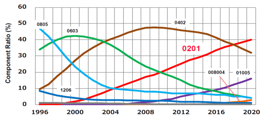
Miniaturisation has continued beyond the smallest sizes described in the original version of this article. Murata announced a 006003-inch MLCC development measuring 0.16 mm × 0.08 mm × 0.08 mm on 19 September 2024. The same announcement identifies its earlier 008004-inch product as 0.25 mm × 0.125 mm and states that it was brought to market in 2014. These dimensions and dates refer to that manufacturer’s products; an announced development does not establish general availability or suitability for a particular assembly process. [4]
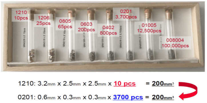
Smaller bodies reduce component volume, but a volume comparison requires length, width and height for both packages. It does not establish equivalent capacitance, voltage capability or assembly yield. The practical limit to downsizing can instead be effective capacitance, board-assembly capability, inspection, rework, mechanical robustness or procurement availability.
Ceramic dielectric classifications
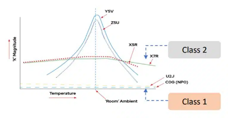
Dielectric composition determines how polarisation responds to electric field and temperature. Class 1 ceramics are approximately linear, low-loss dielectrics intended for applications requiring stability. Class 2 ceramics use high-permittivity ferroelectric materials, commonly based on barium titanate, to obtain greater capacitance in a given volume. The increased permittivity comes with stronger dependence on voltage, temperature and time. [1]
Class 1 compositions are not limited to titanium dioxide: commercial formulations also include other ceramic systems, including calcium zirconate. Similarly, a Class 2 temperature code does not identify a unique chemical formulation. Manufacturers can meet the same temperature-characteristic designation using constructions with different bias dependence and loss. [1,6]
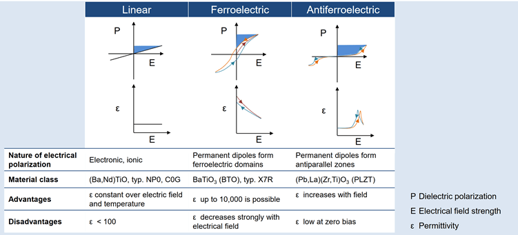
Antiferroelectric materials form a separate material category in the comparison in Figure 8. Their field-dependent polarisation must not be interpreted as a general selection rule that capacitance always increases with applied voltage. For an actual component, use the manufacturer’s charge, capacitance, loss and operating-field data. The Class 1 and Class 2 recommendations in this guide concern the conventional ceramic capacitor families identified by their supplier specifications.
Historical IEC and EIA literature does not use every class label identically. In particular, older EIA Class III terminology appears in discussions of high-permittivity materials such as Z5U and Y5V. Avoid relying on an isolated class number when purchasing or qualifying a part: specify its temperature characteristic, rated voltage, initial tolerance and other required performance limits. Table 2 summarises the practical distinction used in this guide rather than attempting to equate every historical classification.
| Dielectric family | Principal behaviour | Typical design role |
|---|---|---|
| Class 1, including C0G or NP0 | Low loss and high capacitance stability; no appreciable ferroelectric DC-bias loss or logarithmic aging of the type associated with Class 2 ceramics | Resonant circuits, matching, stable filters, timing and precision signal paths |
| Class 2, including X5R and X7R | Higher capacitance density; capacitance depends on temperature, DC bias, AC excitation and time | Decoupling, bypassing, smoothing and coupling where the effective-capacitance range is acceptable |
| High-permittivity temperature characteristics, including Z5U and Y5V | Large permitted temperature variation in addition to voltage and time dependence | Applications that tolerate a wide capacitance range; not a substitute for a stable dielectric merely because nominal capacitance matches |
Construction and Manufacturing Process
Ceramic capacitor manufacture combines ceramic-powder processing, electrode formation, firing and termination. In an MLCC, the dielectric and internal electrodes form a monolithic body, while the external terminations connect the alternating electrode groups to the circuit. Manufacturing controls influence capacitance, insulation resistance, mechanical integrity and long-term reliability. [2,3]
Single-layer and tubular construction
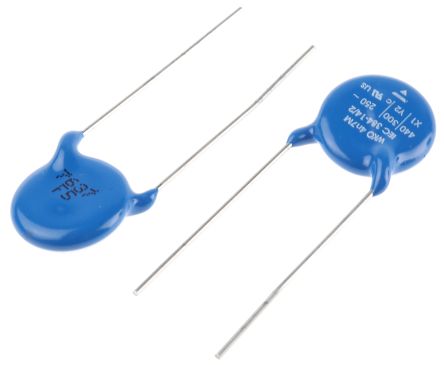
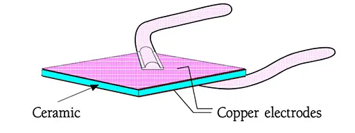
A single-layer capacitor places an electrode on each side of a ceramic dielectric. Leaded disc versions add wire connections and a protective coating; unencapsulated RF versions may instead provide metallised surfaces suitable for bonding. Tubular constructions use the inner and outer surfaces of a ceramic tube as the electrode locations. The metallisation and attachment process depend on the ceramic, voltage, connection method and operating environment.
MLCC manufacturing sequence
Manufacture begins with a controlled ceramic formulation. Ceramic powder is dispersed with binders, solvents and other processing additives to form a slurry. The slurry is cast into thin unfired sheets, usually called green sheets, and dried sufficiently for subsequent processing. Material purity, dispersion, sheet uniformity and contamination control are important throughout this sequence. [2]
The basic green-sheet process comprises sheet formation, internal-electrode printing, stacking, pressing and cutting. Different production arrangements can use carrier films or other sheet-handling methods. Historical descriptions of wet and dry processing explain earlier manufacturing approaches, but do not establish a present-day minimum dielectric thickness or a universal reliability threshold.
A metal paste is printed onto each ceramic sheet to form an internal-electrode pattern. The printed sheets are stacked so that successive electrode groups extend towards opposite ends of the future capacitor. Pressing consolidates the stack, which is then divided into individual unfired chips. The ceramic sheets remain the dielectric; the printed metal becomes the electrodes. [2]
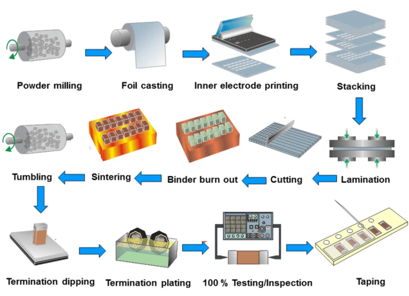
Binder removal precedes final densification of the ceramic. The firing profile and atmosphere must be compatible with both the dielectric and electrode metal. The resulting body is then processed to connect the exposed electrode groups at the two ends. Electrical testing and packaging complete the manufacturing sequence. Firing temperatures and process times are formulation-specific and should not be treated as common specifications for all MLCCs. [2]
The number of active layers, electrode overlap area and dielectric thickness determine the nominal capacitance together with the material permittivity. For equal active gaps and a simplified parallel-plate model, the relationship is given by Eq. (1).
Here C is capacitance, N is the number of active dielectric gaps connected in parallel, ε0 is the vacuum permittivity, εr is relative permittivity, A is the overlapping electrode area of one gap and td is dielectric thickness. The model neglects margins, fringing and differences between layers. For a Class 2 dielectric, εr is not constant across operating conditions, so Eq. (1) is a construction model rather than a complete prediction of in-circuit capacitance.
Layer count is therefore not a stand-alone measure of quality or capability. Nor does a specified capacitance identify the number of layers used: manufacturers can change the ceramic formulation, layer thickness, electrode overlap and body height while retaining the same nominal capacitance and package code.
BME and PME internal electrodes
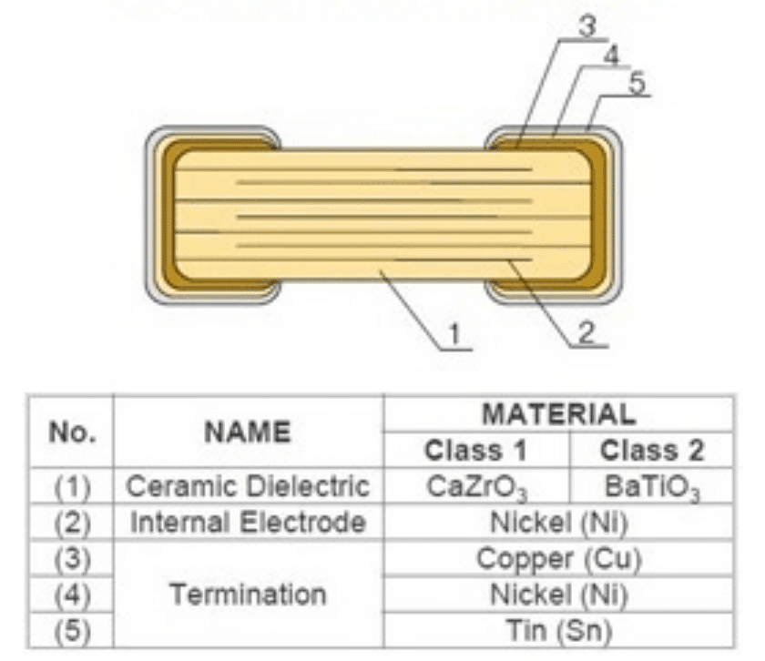
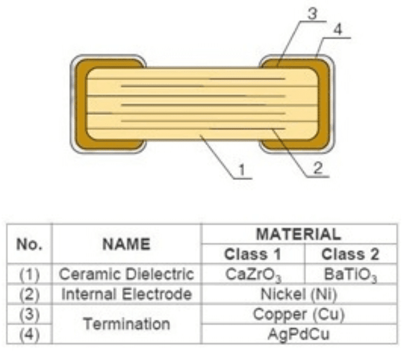
Base metal electrode, or BME, construction commonly uses nickel internal electrodes. Precious metal electrode, or PME, construction uses precious-metal systems such as silver–palladium. These terms describe the electrode technology and must not be confused with the complete external termination stack. For example, a nickel-electrode MLCC can use a copper-based external termination followed by nickel and tin plating. [2,5]
The move towards BME reduced dependence on expensive precious metals and supported high-volume, high-capacitance manufacture. PME remains relevant where the specified product family, qualification or application requires it. However, high-reliability and space-related offerings include both BME and PME technologies; electrode metal alone does not determine whether a component is acceptable for a mission. [9]
Delamination and manufacturing integrity
Delamination is separation within the layered structure. Potential contributors include processing defects, inappropriate binder-removal conditions and stresses associated with the materials and thermal cycle. It is distinct from a board-flex crack, although both can impair insulation and reliability.
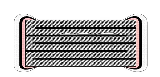
A high capacitance in a small case does not prove that delamination is inevitable, and an electrically functional part should not be assumed reliable merely because a suspected internal separation has not yet caused failure. Acceptance depends on the product specification, qualification and inspection criteria. High-reliability suppliers can provide additional screening and physical-analysis services, but the appropriate method depends on the defect being investigated. [9]
The engineering trade-off behind the original chip-size recommendation remains useful: moving to a different case size can change dielectric thickness, layer count, voltage dependence and mechanical behaviour. However, a universal percentage below the maximum catalogue capacitance is not a valid acceptance criterion. Compare the actual alternatives at the required bias, temperature and assembly conditions.
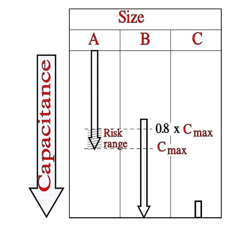
For high-field, shock or vibration applications, review the complete component and mounting arrangement rather than assuming that the largest available case is always preferable. A larger body can provide electrical benefits while also experiencing greater stress from board bending or differential thermal expansion. Flexible terminations, lead frames or different mounting locations may address the mechanical requirement more effectively. [3,5,6]
External terminations and solderable finishes
The external termination makes electrical contact to the internal electrode group and provides a connection to the assembly. A common nickel-electrode construction uses a copper-based termination, a nickel barrier layer and an outer tin finish. The nickel layer limits interaction with solder, while the outer finish supports solderability. Other stacks are available for particular attachment methods and reliability requirements. [2,9]
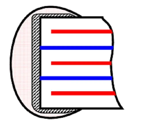
Electroplated and hot-dipped finishes can have different thickness distributions and surface profiles. Finish composition, plating controls, barrier integrity, storage and soldering compatibility all matter. There is no single termination-layer thickness prescription that can replace the supplier’s controlled specification.
For procurement, identify the complete termination option, not merely the nominal capacitor value and case size. Tin, tin–lead, noble-metal and conductive-adhesive-compatible finishes are not automatically interchangeable. Long storage, corrosive atmospheres and unsuitable packaging can degrade solderability; follow the supplier’s storage guidance and confirm solderability when required. [3,9]
Flexible terminations and reduced short-circuit risk
A flexible or soft termination introduces a compliant conductive layer into the termination structure. Its purpose is to reduce the mechanical stress transferred from the PCB and solder joint into the brittle ceramic body. Conductive-polymer systems are one implementation; the exact construction and performance are product-specific. [5]
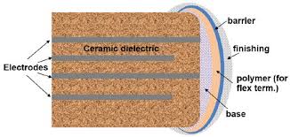
Board flex can arise during depanelisation, connector insertion, screw tightening, test probing, enclosure assembly or operation. Component placement, board support, solder-fillet geometry and assembly tooling remain important even when flexible terminations are used. A soft termination reduces one stress-transfer mechanism; it does not remove the need to control board strain. [3,5]
Published bend-test displacement is meaningful only with its test geometry, board construction, component orientation and acceptance criteria. KYOCERA AVX reports 5 mm board-bend performance for the FlexiTerm construction discussed in its technical paper. That result must not be generalised to every flexible-termination MLCC or treated as an allowable deflection for an arbitrary production board. [5]
Distinguish three different design measures: a compliant termination reduces stress transfer; an open-mode electrode arrangement reduces the likelihood that a particular crack bridges opposite polarities; and a series or floating-electrode arrangement can retain an insulating section if another section is damaged. These measures may be combined, but they are not equivalent. A preferred open failure under a defined flex test is not a guarantee of open failure under electrical overstress or every possible crack path. [5,6]
High-voltage surface-mount ceramic capacitors
High-voltage MLCCs can resemble lower-voltage parts externally while using different dielectric thicknesses, electrode patterns, margins or surface-field controls. The boundary between medium-voltage and high-voltage products varies between suppliers, so the label is less useful than the actual voltage rating, waveform limits and environmental conditions.
Both C0G and X7R high-voltage constructions are available. Their temperature-characteristic names do not make their power-handling behaviour equivalent: Class 2 capacitance can decrease substantially under DC bias, while dielectric loss and electromechanical effects can become important under AC or pulse excitation. Check capacitance at the operating bias as well as the voltage and thermal limits. [3,6]
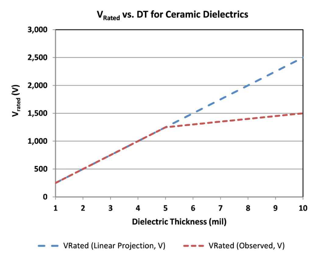
Increasing dielectric thickness reduces electric field for a given layer voltage, but also reduces capacitance per active gap. Within an approximately fixed active volume, fewer thicker gaps can fit, so capacitance density can fall faster than the capacitance of one isolated gap. The original relationship illustrations are retained in Figures 20 and 21.
Figure 20. Original capacitance relationship accompanying the high-voltage construction discussion.
Here:
- C is capacitance (F).
- Vol is volume (m³).
- ε0 is the permittivity of free space, approximately 8.854 × 10⁻¹² F/m.
- ε′ is the real part of the relative permittivity of the dielectric between each electrode pair (dimensionless).
- n is the number of active dielectric layers in the MLCC.
- An is the electrode overlap area per active layer.
Figure 21. Relationship illustration for capacitance density and dielectric thickness.
For an idealised stack in which electrode thickness and inactive margins are neglected, capacitance per dielectric volume varies approximately with the inverse square of dielectric thickness. This is a geometrical scaling argument, not a universal voltage-rating equation. Actual products also depend on electrode thickness, ceramic formulation, electric-field concentration, margins and external insulation.
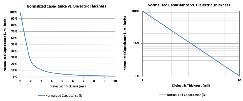
Rated voltage must not be inferred from a universal volts-per-micrometre rule. Breakdown strength, long-term endurance and surface discharge are different constraints. Internal dielectric thickness alone does not determine how the assembled capacitor behaves in air, humidity, contamination or a coated PCB environment. [3,6]
Floating-electrode or cascade constructions create multiple capacitor sections in series within one ceramic body. The total voltage is distributed between these sections, reducing the voltage applied to an individual dielectric section under the assumed voltage-sharing conditions. The construction trades active overlap and capacitance against voltage capability and, in some designs, improved behaviour for particular crack paths. [6]
In Eq. (2), Ctotal is the terminal capacitance, m is the number of series sections, Cj is the capacitance of section j and Cs is the capacitance of each section when all are equal. For equal sections, equal division of an applied voltage is the ideal model; actual sharing and qualification remain properties of the complete design. The number of floating electrodes must not be substituted for m without examining the electrode arrangement.
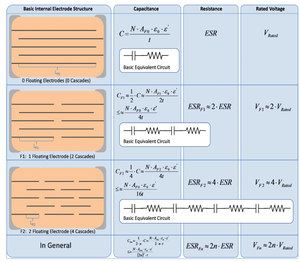
ESR does not follow a single multiplier across all floating-electrode parts. Added series sections increase resistance if everything else is unchanged, but manufacturers can also alter electrode area, current-path length, material and the number of parallel layers. Compare measured or modelled impedance and ESR for the exact part at the application frequency. [6]
External arcing requires separate attention. Terminal spacing, electrode shielding, board cleanliness, humidity, coating and the surrounding conductor layout affect the electric field outside the ceramic. A coating is not automatically sufficient: its compatibility with the component, assembly process and insulation requirements must be established. [3,6]
For mains-connected EMI suppression or another safety-critical insulation position, select an appropriately approved capacitor for the required X or Y function and applicable equipment standard. IEC 60384-14 addresses capacitors for interference suppression and connection to the supply; its 2023 edition and subsequent amendment history must be distinguished from a generic high-voltage DC rating. Automotive stress qualification does not replace this safety approval. [7,8]
Other Construction Types
Specialised ceramic and related inorganic-dielectric capacitors modify electrode geometry, connection method or packaging to meet requirements that a conventional two-terminal chip may not satisfy. Important examples include RF thin-film devices, low-inductance layouts, leaded or stacked assemblies and discoidal feedthrough capacitors. Select these variants by their electrical model and mounting requirements, not by appearance alone.
RF thin-film capacitors
Thin-film RF capacitors use controlled deposited films and patterned electrodes to obtain precise geometry and repeatable electrical behaviour. They may occupy chip packages resembling MLCCs, but the package outline does not make them multilayer ceramic capacitors. Likewise, a device using an inorganic thin-film dielectric should not automatically be assigned the properties of a conventional sintered Class 1 ceramic.
Relevant RF selection parameters include capacitance tolerance, Q, ESR, self-resonant frequency, repeatability and the available S-parameter model. Thin-film products can provide tight tolerances and low RF losses, while suitable multilayer RF capacitors remain alternatives where their capacitance range, power handling or assembly format is preferable. [9]
A repeatable principal resonance can be valuable in matching and filter design, but no real capacitor should be assumed to have only one resonance at every frequency. Package parasitics, mounting and distributed behaviour remain important. For a band-reject or narrow-band matching network, compare the installed response over the complete frequency range rather than choosing solely from nominal capacitance.
Low-ESL designs
Equivalent series inductance, abbreviated ESL, limits the usefulness of a capacitor at high frequency. Changing the electrode arrangement and terminal locations can shorten current paths or reduce their magnetic loop area. Reverse-geometry, multi-terminal and feedthrough arrangements therefore provide alternatives to a conventional two-terminal rectangular chip.
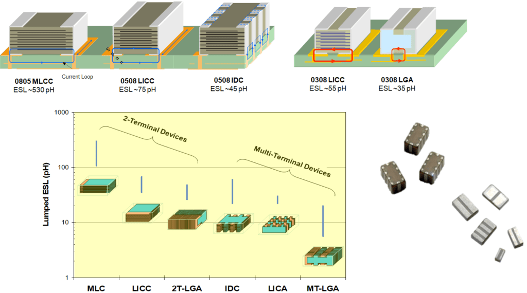
For power-distribution decoupling, the capacitor is only part of the current loop. Pads, vias, planes and distance to the load add inductance, so an electrically low-inductance component can perform poorly if its PCB connection is unsuitable. Compare the complete mounted impedance and check for resonances when several capacitor values or technologies are combined.
For signal coupling, also check the required passband, return loss and connection geometry. A low-ESL power-decoupling construction is not automatically the correct component for a controlled-impedance high-speed signal path.
Leaded and stacked MLCCs
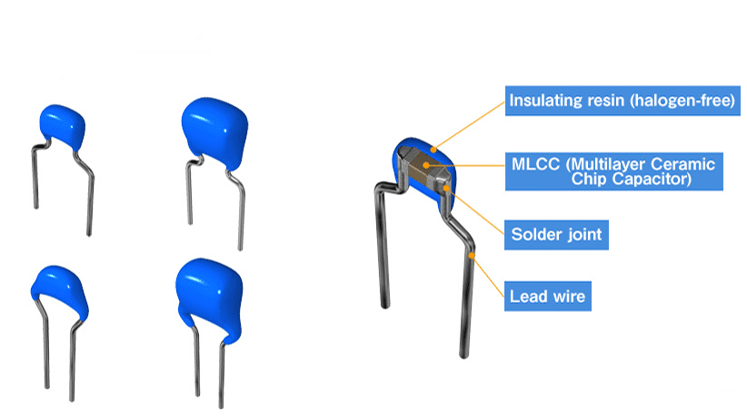
Leaded MLCCs include encapsulated radial or axial components and chip assemblies mounted on compliant terminals or frames. A lead can provide through-hole compatibility or mechanical isolation from the PCB. Stacking several ceramic chips can increase total capacitance while using a frame to accommodate attachment and mechanical requirements. [6,9]
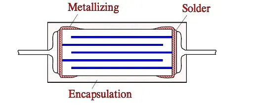
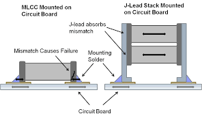
These arrangements can be useful for larger capacitances, higher-voltage circuits or demanding mechanical environments. However, added leads and frames also change inductance, resistance, vibration response, mounting clearance and heat transfer. Mechanical compliance must be evaluated with the complete assembly and its mounting, rather than inferred solely from the presence of leads. [6,9]

Discoidal and feedthrough capacitors
A discoidal capacitor uses a concentric geometry, commonly with a central opening for a conductor. In a feedthrough arrangement, this geometry provides a short connection from the conductor to a surrounding reference or enclosure. It is useful in filtered connectors and other EMI-control assemblies where the physical current path is part of the filtering function.
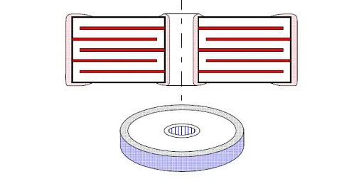
The installed filtering response depends on the connection to the enclosure or reference plane, not just the capacitor’s measured low-frequency value. Also check the dielectric’s bias dependence, the conductor’s current capability, attachment stresses and any sealing or environmental requirements. A feedthrough configuration does not, by itself, establish a safety-insulation rating.
Failure Modes and Assembly Reliability
MLCC reliability depends on manufacturing integrity, electrical stress, environmental exposure and assembly strain. Mechanical cracks are particularly important because a capacitor may initially pass a capacitance check and subsequently develop insulation degradation. Expected Class 2 capacitance changes under bias or aging must be distinguished from physical damage or dielectric breakdown. [3,5]
Flex cracks, leakage and short circuits
A board-flex crack often begins near the termination-to-ceramic region, where the soldered connection transfers strain into the body. If the crack reaches active electrode layers, it can reduce insulation resistance or create a short circuit. Moisture entering a crack can contribute to delayed electrical degradation, so an apparently satisfactory capacitance measurement does not rule out damage. [5]
In a high-impedance signal circuit, leakage may cause offset, drift or loss of signal integrity before an obvious short develops. On a low-impedance power rail, a conductive fault can draw substantial current and cause local heating. The consequence therefore depends on the circuit’s available fault energy as well as the component defect. [5]
Do not rely on increased voltage or fault current to burn away a conductive path. MLCCs are not designed as self-healing metallised-film capacitors, and an apparently cleared fault can remain damaged. Failure containment belongs in the circuit architecture, protection and component-selection process.
Thermal shock and soldering damage
Rapid or uneven heating and cooling can produce internal stress. Potential sources include an unsuitable reflow profile, wave soldering outside the permitted process window, local rework and immersion in a much cooler cleaning medium. Thermal cracking is therefore not confined to direct contact with a soldering iron. [3]
- Use the supplier’s permitted mounting process for the exact series and package.
- Control preheating, temperature differential, peak temperature, time and cooling rather than relying on a generic package-size rule.
- Avoid contacting the ceramic body with a soldering-iron tip; follow the specified rework method and support the board.
- Control solder volume and fillet geometry. Excess solder can increase mechanical coupling to the PCB.
- Qualify cleaning and coating processes, including ultrasonic cleaning where used, for their mechanical and chemical effects.
Neither a nickel barrier nor a particular body size establishes that reflow, vapour-phase or hot-air soldering is risk-free. The acceptable process is a property of the specified component and assembly, and larger devices may need additional mechanical precautions. [3]
Solderability, leaching and storage
Oxidation, contamination or corrosive storage conditions can impair solderability. Excessive soldering time or temperature can also cause termination leaching or loss of adhesion. Barrier-layer design helps control interaction with solder, but does not compensate for an unsuitable process. [3]
Keep components in the manufacturer’s protective packaging and observe its storage conditions and permitted storage period. Review aged stock before use, including solderability testing where required. For sensitive termination systems, confirm compatibility with packaging materials and the local atmosphere rather than assuming that any unsealed storage container is acceptable. [3]
Electrical overstress and ripple heating
Dielectric breakdown can produce a short circuit. Evaluate the maximum terminal waveform, including DC, ripple, startup, switching overshoot and abnormal transients, against the supplier’s voltage rules. A DC voltage rating must not be converted into an AC or repetitive-pulse rating by a simple numerical substitution. [3]
AC and repetitive pulse currents cause loss and self-heating. The permissible operating point depends on frequency, waveform, dielectric, capacitance, construction, heat transfer and ambient temperature. Class 1 capacitors are often advantageous where low dielectric loss and stable capacitance are important, but they still require their own voltage, current and thermal checks. Class 2 ceramics are not categorically restricted to isolated pulses; suitability depends on the specified application limits. [3,6]
Screening, qualification and failure analysis
Additional screening can reduce risk for a defined application, but no single electrical or imaging test detects every defect. Select inspection and acceptance criteria according to the governing component specification and the relevant failure mechanisms. Available services can include destructive physical analysis, X-ray inspection, ultrasonic scanning and electrical stress testing. [9]
For automotive use, AEC-Q200 defines stress-test qualification requirements for passive components. It does not provide a certification board, and supplier qualification does not remove the user’s responsibility to validate suitability for the intended application. Review the qualification revision, covered product family, construction, manufacturing location and any customer-specific requirements. [7]
For space, defence or other high-reliability equipment, use the applicable approved component specification, screening level and project requirements. Do not infer suitability from a generic high-reliability label, electrode metal or price premium. Likewise, do not substitute automotive qualification for mains-safety approval or another required insulation qualification. [7–9]
Class 1 Ceramic Capacitors
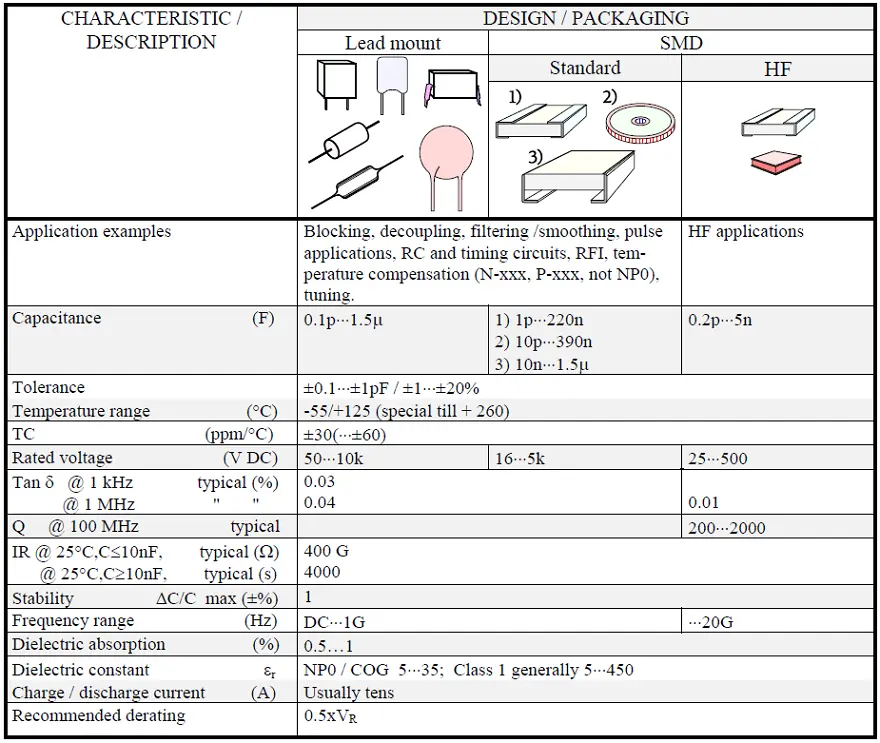
Class 1 ceramic capacitors prioritise predictable capacitance and low loss rather than maximum capacitance density. They are appropriate for resonant circuits, RF matching, stable filters and other applications where changes in capacitance would directly affect performance. C0G, commonly also called NP0, is a widely used near-zero-temperature-coefficient characteristic within this family. [1,10,14]
Temperature coefficient and capacitance tolerance
Class 1 includes both near-zero and intentionally non-zero temperature coefficients. An approximately linear coefficient can compensate for the temperature dependence of another circuit element. Traditional designations such as P100, N150 and N1500 indicate nominal positive or negative coefficients of 100 ppm/°C, 150 ppm/°C and 1,500 ppm/°C respectively; their permitted deviations and operating ranges must be taken from the applicable specification.
C0G specifies a nominal coefficient of zero with a permitted deviation of ±30 ppm/°C. The middle character is the digit zero, not the letter O. The coefficient describes temperature dependence, not initial capacitance tolerance: a capacitor can have a small temperature coefficient while still having a comparatively wide initial tolerance. [14]
In Eq. (3), C(T) is capacitance at temperature T, C(Tref) is capacitance at reference temperature Tref, and αC is the capacitance temperature coefficient expressed as a fractional change per degree. Convert a coefficient in ppm/°C by multiplying it by 10−6. The equation assumes an approximately linear characteristic and does not include initial tolerance or other sources of drift.
For example, a 100 °C increase from 25 °C to 125 °C produces a maximum coefficient contribution of approximately ±0.3% for a ±30 ppm/°C characteristic. A nominal N150 coefficient produces a −1.5% change over the same temperature difference before its coefficient tolerance is considered. These are coefficient calculations, not complete worst-case component tolerances.
At small capacitance values, an absolute tolerance is often more informative than a percentage. At a nominal 10 pF, absolute tolerances of ±0.1 pF, ±0.25 pF, ±0.5 pF and ±1 pF correspond to ±1%, ±2.5%, ±5% and ±10% respectively. Available tolerances depend on the product family, nominal value and manufacturing process; the examples are mathematical comparisons rather than a claim that every option is available for every part.
Some historical precision constructions used electrode trimming to adjust capacitance. A filled trimming feature should be evaluated against the manufacturer’s construction drawing rather than automatically classified as a void or delamination. For failure analysis, the intended construction and the acceptance criteria must be established before drawing conclusions from a sectioned sample.
Dielectric absorption and precision applications
Low dielectric loss does not mean zero dielectric absorption. Dielectric absorption describes delayed polarisation relaxation that can produce voltage recovery after a capacitor has been charged, discharged and then left open-circuit. Its measured magnitude depends on the charging, discharge and recovery intervals as well as the material. [10]
For precision integrators, sample-and-hold circuits and other charge-sensitive signal paths, evaluate absorption and leakage separately from dissipation factor. Do not assign a single dielectric-absorption percentage to every Class 1 formulation. Further background is provided in the explanation of dipoles and dielectric absorption.
RF and microwave ceramic capacitors
RF capacitor selection requires more than a C0G designation. Electrode conductivity, dielectric loss, terminal geometry, mounting inductance and distributed resonances all influence the usable frequency range. Specialised ceramic and porcelain formulations, single-layer constructions and thin-film devices address different combinations of Q, capacitance, power handling and package size. [9]
There is no universal frequency above which all conventional MLCCs become unsuitable. Compare frequency-dependent ESR, Q, impedance and the relevant RF model for the exact device. For power RF, also check the permitted RF voltage, current and temperature rise; small-signal Q alone does not establish power capability.
Measurement conditions
Measure capacitance and dissipation factor at the frequency, AC voltage and temperature specified for the selected product. Fixture compensation, connection geometry and the instrument’s equivalent-circuit model become particularly important at low capacitance or high frequency. Insulation-resistance and dielectric-withstand measurements have separate voltage, timing and current-limiting requirements. [3,10]
| Capacitance (pF) | Frequency | Measuring voltage (V RMS) |
|---|---|---|
| ≤1,000 | 1 MHz | US MIL: 1 IEC/CECC: 1 |
| >1,000 | 1 kHz | US MIL: 1 IEC/CECC: 1 |
A current limit stated for an insulation or withstand test is not necessarily the permissible current in normal service. Conversely, a capacitor surviving a higher-current experiment does not establish an unrestricted surge rating. For pulse applications, use supplier-approved limits for waveform, voltage slope, peak current, repetition rate and temperature. [3]
Temperature dependence of capacitance, loss and insulation resistance
Figures 34 and 35 retain the original illustrations of capacitance, dissipation factor and insulation resistance versus temperature. They show the types of characteristic that should be examined; their plotted values are not guarantees for other formulations or component families.
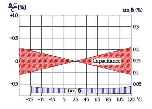
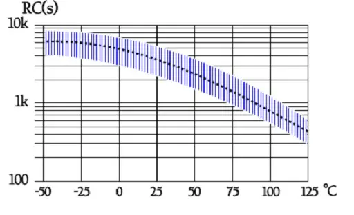
Insulation resistance is often specified using both a resistance limit and a resistance–capacitance product. The latter has units of seconds because an ohm multiplied by a farad equals a second. The applicable datasheet wording determines how these limits combine. [10]
In Eq. (4), RIR is insulation resistance and τIR is its product with capacitance C. Retaining the original calculation, a product of 4,000 s and a capacitance of 10 nF give RIR = 400 GΩ. The arithmetic is correct, but the 4,000 s value is an illustrative input, not a universal Class 1 specification.
Do not extrapolate that example into an unlimited resistance increase as capacitance falls. Surface leakage, fixture leakage and the separately specified resistance limit can become dominant. At very high resistance, control contamination, humidity, guarding, settling time and instrument capability before interpreting the measurement.
Frequency dependence and quality factor
Capacitance, loss and terminal impedance depend on frequency. At sufficiently high frequency, a single lumped capacitance is no longer a complete description of the component. The original curves below illustrate these dependencies for particular constructions.
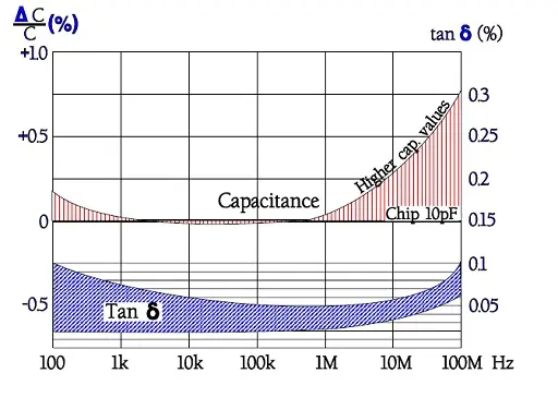
For a capacitor operating below self-resonance in an appropriate equivalent-series model, quality factor Q is the reciprocal of dissipation factor tan δ. Eq. (5) relates it to capacitance and ESR. [10]
Here f is frequency, C is the capacitance appropriate to that frequency and test condition, and ESR is equivalent series resistance at the same condition. The approximation treats the device as a series resistance and capacitance with negligible inductive reactance. Near resonance, use the full impedance or RF model rather than extending this expression beyond its assumptions.
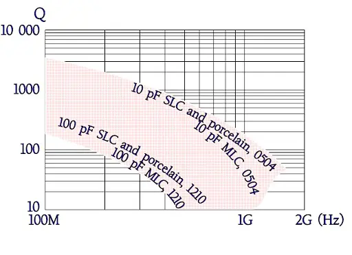
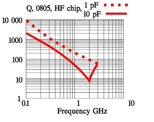
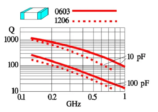
For a given family, smaller capacitance or a different case size can improve Q over part of the frequency range. That trend is not a universal ranking: changing the package can also change electrode resistance, inductance and the location of resonances. Compare parts at the actual operating frequency and mounting reference plane.
ESR and terminal impedance
ESR represents losses in an equivalent circuit at a specified frequency. It includes contributions from the electrodes, terminations and dielectric, and it should not be treated as a frequency-independent material constant. Figures 40–43 retain the original examples of ESR and impedance behaviour. [10]
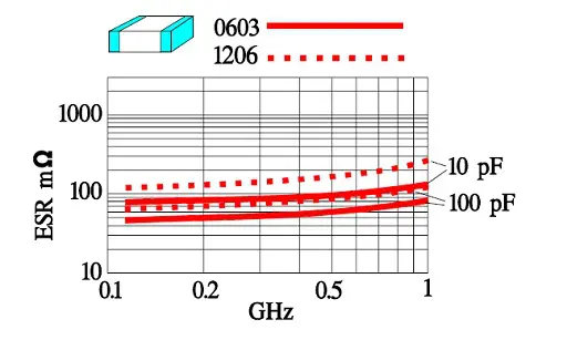
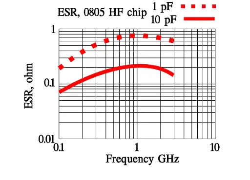
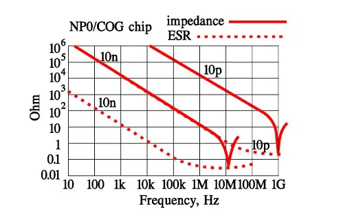
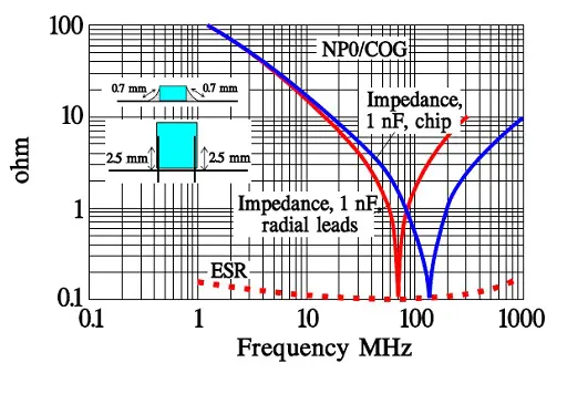
Leads and mounting connections add inductance, which can shift the useful frequency range even if the dielectric and nominal capacitance are similar. For RF and fast decoupling, include the PCB connection in the model. For repetitive power duty, also evaluate losses and temperature rise rather than interpreting low impedance as unlimited current capability. [3,10]
Self-resonant frequency
In the simplest series model, self-resonance occurs when capacitive and inductive reactances cancel. Eq. (6) gives the corresponding frequency. Real devices and mounted networks can have additional resonances, so this equation identifies a first-order relationship rather than a complete high-frequency model. [10]
Here f0 is the series-resonant frequency and Ls is the series inductance associated with the chosen component and connection reference plane. Increasing capacitance lowers this resonance if inductance remains unchanged; reducing connection inductance raises it. Above the first series resonance, the simple model becomes predominantly inductive.
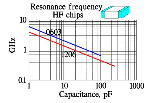
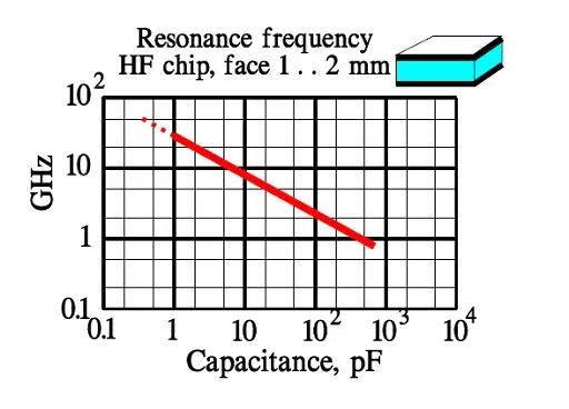
The comparison between Figures 44 and 45 illustrates why construction matters alongside external dimensions. It should not be used to assign a universal resonance advantage to every single-layer or multilayer part. Compare supplier impedance or S-parameter data for the selected alternatives under compatible mounting conditions.
Class 2 Ceramic Capacitors
Class 2 ceramic capacitors obtain high capacitance density from high-permittivity ferroelectric formulations, commonly based on barium titanate. They are useful for bypassing, decoupling and smoothing when their operating capacitance range is acceptable. Their capacitance must be evaluated as a function of temperature, applied voltage, excitation and time, not as an invariant catalogue value. [1,3,10]
Temperature-characteristic codes
The familiar three-character code identifies a lower temperature, an upper temperature and a permitted capacitance change over that interval under the specified reference conditions. It is not an initial-tolerance code, a DC-bias specification or an aging-rate specification. Table 5 retains the original code-decoding structure. [10]
| First character: lower temperature | Second character: upper temperature | Third character: capacitance change |
|---|---|---|
| X = −55 °C | 4 = +65 °C | P = ±10% |
| Y = −30 °C | 5 = +85 °C | R = ±15% |
| Z = +10 °C | 6 = +105 °C | S = ±22% |
| Not applicable | 7 = +125 °C | T = +22% / −33% |
| Not applicable | 8 = +150 °C | U = +22% / −56% |
| Not applicable | 9 = +200 °C | V = +22% / −82% |
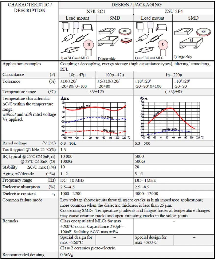
X7R therefore identifies a −55 °C to +125 °C interval with capacitance change within ±15% under the specified temperature-characteristic test. X5R uses the same ±15% change limit over −55 °C to +85 °C. Z5U permits +22% / −56% over +10 °C to +85 °C, while Y5V permits +22% / −82% over −30 °C to +85 °C. The latter characteristics can be unsuitable where a minimum capacitance must be maintained across a wide temperature range. [10]
Do not combine the X7R temperature band with initial tolerance and then assume that all voltage effects are included. The EIA temperature designation does not guarantee the capacitance remaining under DC bias. Likewise, moving from X5R to X7R extends the coded temperature interval but does not, by itself, guarantee better DC-bias behaviour. [1,3,10]
| Specification | Class | Temperature range (°C) | ΔC/C (%) at VC = 0 | ΔC/C (%) at VC = VR |
|---|---|---|---|---|
| EIA | X7R | −55 to +125 | ±15 | — |
| CECC | 2C1 | −55 to +125 | ±20 | +20 / −30 |
| CECC | 2X1 | −55 to +125 | ±15 | +15 / −25 |
| MIL | BX | −55 to +125 | ±15 | +15 / −25 |
| MIL | BZ | −55 to +125 | ±20 | +20 / −30 |
| EIA | Z5U | +10 to +85 | +22 / −56 | — |
| CECC | 2F4 | −25 to +85 | +30 / −80 | +30 / −90 |
| BS | 2F4 | −25 to +85 | +30 / −80 | — |
Historical designations such as 2C1, 2F4 and MIL characteristic codes can include requirements that differ from an EIA temperature code. A cross-reference table is not sufficient evidence of full interchangeability. Confirm the permitted capacitance change under the relevant temperature and voltage conditions in the controlled specification.

The coded interval is not permission to operate a part outside its specified temperature range. Do not assume that a Z5U part is acceptable at −55 °C merely because the ceramic may survive the exposure. Electrical limits, coating, terminations and the complete component qualification still apply.
Measurement conditions and excitation amplitude
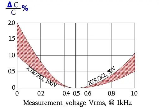
Class 2 capacitance measurements are especially sensitive to AC excitation. Measure at the specified frequency and voltage, and confirm the voltage actually present across the device. An instrument’s source-voltage setting can differ from the terminal voltage when its output impedance and the capacitor’s impedance form a divider. [3]
| Material | Reference | Measuring voltage at 1 kHz |
|---|---|---|
| BX | MIL | 1 V RMS |
| X7R/2C1 | IEC/CECC/Manufacturer | 1 V RMS Sometimes 0.5 V RMS |
| Z5U/2F4 | IEC/CECC/Manufacturer | 1 V RMS Sometimes 0.5 or 0.3 V RMS |
Document AC amplitude as RMS, peak or peak-to-peak, rather than recording an unqualified voltage. Also record DC bias, frequency, temperature, equivalent-circuit mode, fixture compensation, time since heat treatment and bias dwell time. Without compatible conditions, a difference between two measurements need not indicate a defective part. [3,12,13]

Curie transition and ferroelectric behaviour
The Curie transition concerns a change in crystal symmetry and ferroelectric behaviour. For barium-titanate-based systems, the transition separates a ferroelectric state from a paraelectric state; it is not a brittle transition and does not mean that the material ceases to be a dielectric. Composition and microstructure modify the transition and the temperature dependence of permittivity. [11]
The Curie transition must also be distinguished from a component’s maximum operating temperature. A dielectric formulation, termination system and encapsulation are qualified together for a specified operating range. Do not infer that range from a generic Curie temperature or from the behaviour of pure barium titanate.
Charge, voltage and differential capacitance
Ferroelectric polarisation is nonlinear and can exhibit hysteresis. Consequently, the charge associated with a voltage depends on the operating point and the excitation history. Figure 49 retains the original illustration of a ferroelectric charge–voltage loop.
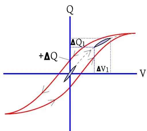
For a sufficiently small perturbation around a defined operating state, differential capacitance is the local slope of the charge–voltage relationship, as expressed in Eq. (7). This explains why a small AC measurement superimposed on DC bias can report much less capacitance than a nominal zero-bias measurement. [13]
Here Q is terminal charge, V is terminal voltage and the state includes temperature and the relevant polarisation history. Frequency and AC amplitude must also be specified for a real measurement. This differential capacitance is not automatically equal to Q/V or to a capacitance inferred from a large charge or discharge excursion.
Hysteresis and dielectric absorption are related to polarisation behaviour, but they are not interchangeable descriptions. A hysteresis loop describes the path dependence of charge and voltage, while an absorption measurement examines recovery after a defined charge and discharge sequence. A Class 2 capacitor can introduce settling errors, distortion and history dependence in a precision signal circuit even when its nominal capacitance and voltage rating appear suitable. [10,13]
DC-bias dependence
Applying DC voltage to a high-permittivity ceramic changes its polarisation response and commonly reduces its small-signal capacitance. The magnitude depends on the formulation and internal construction as well as the applied voltage. The temperature code alone does not specify this loss. [1,3,10]

Neither a higher voltage rating nor a larger case guarantees a particular improvement in capacitance retention. Either can help in a specific product comparison, but manufacturers can obtain the ratings through different combinations of material, layer thickness, overlap and body height. Compare the actual bias curves and their measurement conditions for each candidate.
For a converter, calculate whether the remaining capacitance meets the controller’s input or output requirements and the required transient response. For an LC filter, evaluate the shift in impedance and resonance. For signal coupling or timing, also consider distortion and the dependence on signal amplitude. These are different design questions and may require different capacitance definitions. [3,13]
AC-voltage dependence and repetitive pulses
Changing AC amplitude changes the portion of the nonlinear characteristic being exercised. Capacitance can increase over part of the amplitude range and decrease elsewhere; the response also depends on DC bias, frequency and history. The original statement that AC voltage simply has the reverse effect of DC voltage is therefore insufficient. [10,13]
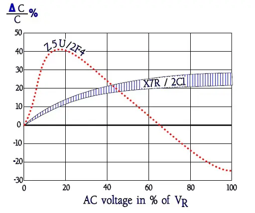
For an approximately memoryless charge–voltage model, the capacitive current follows Eq. (8). The constant-capacitance form is useful for an initial pulse calculation, but a strongly nonlinear or hysteretic device requires a model appropriate to its operating trajectory. [10,13]
Here i(t) is capacitive current, v is instantaneous voltage and t is time. The original example gives 1 A for a constant 1 nF capacitance at 1,000 V/µs. A larger constant capacitance gives a proportionally larger current. This arithmetic does not establish that the capacitor can tolerate that voltage slope or current.
For repetitive pulses, compare peak voltage, peak current, repetition rate, waveform spectrum and temperature rise with the supplier’s limits. Class 2 capacitors are not universally restricted to single pulses, but their dielectric loss and electromechanical response can make them unsuitable for a particular high-energy or resonant duty. A DC rating or a one-off surge test cannot replace an approved repetitive operating limit. [3,6]
Piezoelectric effects, microphonics and acoustic noise
High-permittivity ferroelectric ceramics exhibit electromechanical coupling. An electrical waveform can produce mechanical movement that excites the PCB and becomes audible; mechanical vibration can conversely generate an electrical response. The observed result depends on bias, excitation, construction, mounting and mechanical resonances. [3,6,10]
In low-level analogue circuits, vibration-induced signals can appear as microphonic noise. In power electronics, audible tones can arise when the electrical excitation or its modulation excites the assembly. Do not test this behaviour by striking a capacitor: the impact can create a crack and confound the electrical observation.
Possible mitigations include choosing a dielectric without the same ferroelectric response, selecting a low-acoustic-noise construction, using a mechanically isolating package or changing the PCB placement and support. Validate the complete assembly because a change in the board’s mechanical response can matter as much as a change in the capacitor.
Aging and de-aging
Class 2 capacitance decreases with elapsed time after the dielectric has been thermally reset. This aging is commonly approximated as a specified percentage per decade of elapsed time: 1–10 hours, 10–100 hours and 100–1,000 hours are each one decade. It is not a fixed percentage loss per calendar year. C0G does not exhibit this ferroelectric logarithmic-aging mechanism. [1,11,14]
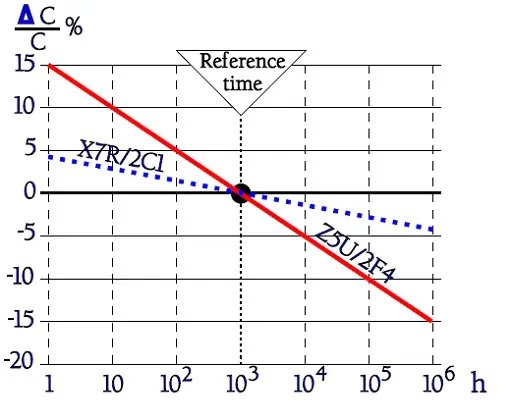
Published aging rates vary between formulations, including products sharing the same temperature code. Use the specified rate and reference convention for the exact product rather than a universal X7R or Z5U constant. As an illustrative calculation, a model using a constant 2% change per time decade relative to its stated reference capacitance gives approximately 6% change over three decades of elapsed time. [10,11]
The elapsed-time origin, reference capacitance and post-heating measurement delay must be defined. A capacitance guaranteed at one reference time is not automatically guaranteed to remain within the initial tolerance throughout the equipment lifetime. Nor is there a universal requirement that every ceramic capacitor’s nominal value is guaranteed specifically at 1,000 hours. [10,11]
Figure 53. Reference-time capacitance formula accompanying the aging discussion.
Heating above the relevant transition under a suitable time–temperature treatment can restore the capacitance towards its de-aged value, after which aging starts again. Soldering can therefore reset the aging history. Use the manufacturer’s specified treatment and recovery interval when comparing measurements; de-aging is a measurement-conditioning process, not a repair for a cracked or electrically damaged capacitor. [10,11]
DC-bias aging and operating history
A voltage step can produce an immediate capacitance change followed by further time-dependent change under bias. This biased evolution should not be assumed identical to the unbiased aging rate measured after a thermal reset. Removing or reducing the bias can produce partial recovery, and the subsequent result depends on the voltage and thermal history. [12]
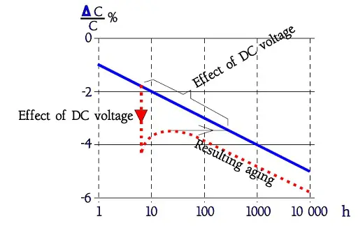
Continental reported an automotive control-unit problem in which capacitance continued to decrease after the initial bias-induced reduction had already been included in the design calculation. Its published engineering response emphasised time-dependent bias data, defined measurement conditions and an application-specific minimum capacitance. This is a practical reason to examine biased dwell time rather than relying exclusively on an immediate room-temperature bias sweep. [12]
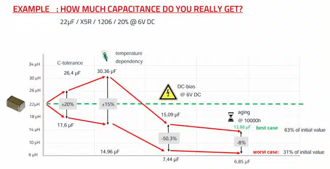
Temperature, DC bias, AC excitation and history interact. A multiplication of separate correction factors can be useful only when the supplier’s data and reference conventions support that treatment. It is not a universal physical law, and combining unrelated typical curves can either miss interactions or count the same effect twice. Prefer a validated combined-condition model or measurement for critical operating points. [3,12,13]
Temperature dependence under DC bias
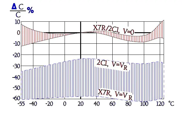
The capacitance–temperature curve under bias can differ from the zero-bias temperature characteristic. Evaluate the operating envelope rather than adding a room-temperature bias percentage to the temperature-code limits without checking compatibility. Figures 56 and 57 retain the original comparisons with and without applied voltage. [3,10]
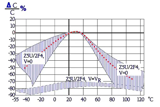
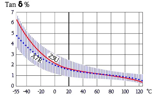
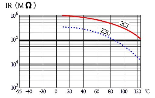
Insulation resistance commonly decreases as temperature rises, but its magnitude and temperature dependence are product-specific. Use the stated minimum at the relevant conditions. A typical curve cannot establish a universal one-decade decrease between room temperature and 125 °C.
Frequency dependence, ESR and impedance
Class 2 capacitance and loss vary with frequency, while electrode and mounting parasitics determine the terminal impedance around and above resonance. The following original figures illustrate the separate quantities that need to be checked; they should not be combined into a model unless they describe the same component and compatible test conditions. [3,10]
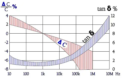
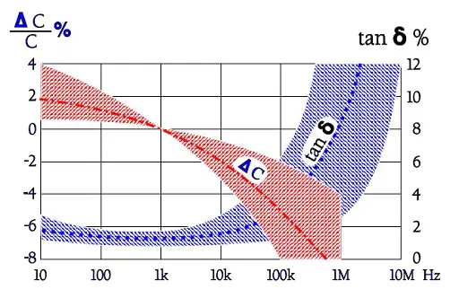

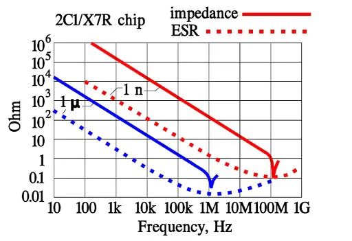
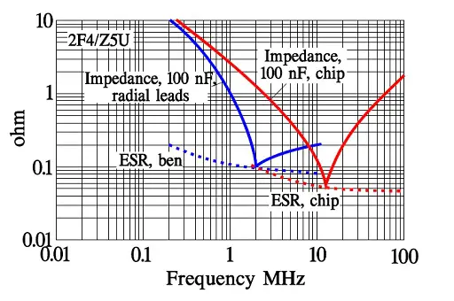
For decoupling and EMI filtering, evaluate the mounted network over the required frequency range. Bias-induced capacitance changes move resonances, and parallel capacitors or series inductive elements can introduce anti-resonant peaks. For power applications, check heating separately; a low impedance minimum does not identify a safe continuous operating current. [3,13]
Small-signal capacitance versus charge and energy
A small-signal capacitance is useful for impedance and local control-loop analysis around a bias point. A large discharge excursion, startup waveform or resonant swing can sample a much wider region of the nonlinear characteristic. The same single capacitance value may therefore be inadequate for all three tasks. [13]
For a reversible, memoryless nonlinear model, the charge and energy changes follow Eq. (9). These integrals illustrate why substituting one biased small-signal capacitance into the constant-capacitance energy formula can be misleading. A hysteretic device requires the actual path and losses to be considered rather than being represented by a unique voltage-only stored-energy function. [13]
Here ΔQ is charge change, ΔW is energy change in the stated reversible model, and V1 and V2 are the initial and final voltages. For constant C, these reduce to the familiar linear-capacitor relationships. For a practical MLCC, confirm whether the supplier model represents small-signal impedance, charge behaviour, nonlinear transient response or only a subset of these properties.
Design and Selection Checklist
Start with the circuit requirement and the worst operating conditions, then compare exact part numbers. Nominal capacitance, dielectric code, package size and rated voltage are necessary identifiers, but they do not establish electrical, mechanical or sourcing equivalence. The following checklist separates the principal application classes.
| Application | Parameters to prioritise | Validation focus |
|---|---|---|
| Precision signal, timing and stable filters | Temperature coefficient, initial tolerance, voltage coefficient, absorption, leakage and drift | Settling, distortion and accuracy across the intended signal and temperature range |
| RF matching and resonant circuits | Q, ESR, self-resonance, RF voltage and current capability, tolerance and S-parameters | Mounted frequency response, losses and temperature rise at operating power |
| Power-rail decoupling and converter filtering | Effective capacitance under bias and aging, ESR, ESL and ripple capability | Transient response, controller stability, mounted impedance and heating |
| Resonant power conversion and repetitive pulses | Waveform-dependent voltage and current limits, dielectric loss, nonlinearity and electromechanical behaviour | Actual waveform, peak and RMS stress, temperature and endurance |
| EMI feedthrough and filtered connectors | Installed impedance, connection geometry, bias dependence and mechanical integration | Filtering in the intended enclosure and grounding arrangement |
| Safety-related suppression positions | Required X or Y classification, approvals, working voltage and equipment insulation requirements | Approval coverage and compliance of the complete equipment design |
Electrical specification
- Define the required minimum and maximum effective capacitance, not just a preferred nominal value.
- Record DC voltage, ripple amplitude, frequency spectrum, startup, shutdown, overshoot and credible fault conditions.
- Check initial tolerance, temperature dependence, DC and AC voltage dependence, aging and time under bias using compatible reference conditions.
- Identify which data are guaranteed limits, which are typical curves and which are simulation results. Agree additional acceptance requirements where the design cannot tolerate an unspecified margin.
- Compare impedance, ESR, ESL and resonance over the application frequency range, including mounting parasitics.
- Check insulation resistance, leakage, absorption and electromechanical noise where they affect circuit performance.
Ripple, pulse and thermal verification
For an approximately linear sinusoidal operating condition, Eq. (10) provides an initial estimate of AC loss from RMS current. ESR must correspond to the relevant frequency, temperature and operating state. [3,10]
Here PAC is AC power loss and IRMS is RMS current. For a switching waveform, account for its frequency content and any amplitude-dependent loss; one low-level ESR measurement is not a complete large-signal thermal model. Validate capacitor temperature in the intended assembly, including ambient temperature, nearby heat sources and cooling. [3]
For high-voltage parts, also check the supplier’s AC-voltage-versus-frequency restrictions and external insulation requirements. A capacitor can meet a simple estimated temperature-rise target while violating another voltage, field or waveform limit.
Mechanical design and assembly
- Check body height, dimensional tolerances, termination option and land pattern as well as the nominal package code.
- Review board strain during depanelisation, connector insertion, fastening, test probing and equipment operation.
- Consider flexible terminations, open-mode electrode designs or leaded assemblies according to the failure mechanism being controlled.
- Qualify the actual soldering, rework, cleaning and coating processes against supplier guidance.
- Review vibration, thermal cycling, humidity and available fault energy. Avoid treating a preferred failure mode in one test as a guarantee under every stress.
Catalogue parts, custom parts and alternate sources
For catalogue parts, approve the complete manufacturer part number, including termination and qualification suffixes. When approving an alternative, compare effective capacitance and impedance at the same operating conditions, along with dimensions, assembly compatibility, qualification coverage and supplier change-control arrangements.
For custom parts, agree the electrical waveform, thermal environment, mechanical interfaces, measurement conditions, acceptance limits and qualification plan before release. A bespoke nominal capacitance or package drawing is insufficient if the application also depends on a guaranteed capacitance after bias dwell, a particular failure response or an installed RF characteristic.
Automotive qualification, project-specific high-reliability screening and safety approval answer different questions. Confirm the applicable AEC-Q200 revision and qualification evidence for automotive parts; use the required approved specification for space or defence projects; and verify the appropriate X or Y approval for safety-suppression positions. None of these labels removes the need for application validation. [7–9]
Conclusion
Ceramic capacitor selection begins with a distinction between construction and dielectric behaviour. MLCC construction provides many active layers in a compact body; Class 1 and Class 2 materials determine very different balances between capacitance density, stability, loss and nonlinearity.
Use Class 1 where predictable capacitance and low loss dominate. Use Class 2 where its higher capacitance density is useful and the effective operating range has been demonstrated. In both cases, qualify the complete part and its mounting for the actual waveform, temperature, mechanical environment and required approvals rather than relying on nominal capacitance and voltage rating alone.
FAQ
These answers summarise the construction, selection and reliability distinctions most relevant to engineering and procurement.
An SLCC has one active ceramic dielectric layer, while an MLCC connects multiple active layers in parallel within one body. Multilayer construction increases capacitance in a compact footprint. Single-layer devices remain useful for specialised RF, microwave, high-voltage and feedthrough functions. Neither construction alone determines dielectric stability, loss, qualification or suitability for a particular circuit.
Choose C0G when stable capacitance, low loss and low voltage dependence are important, such as in matching networks, resonant circuits and precision filters. X7R provides higher capacitance density but changes with voltage, temperature and time. Compare the capacitance actually needed in operation rather than assuming that a larger nominal X7R value provides equivalent performance.
In a Class 2 ferroelectric dielectric, an applied DC field changes the polarisation response to a small AC signal. The resulting measured capacitance can be substantially below its nominal value. The loss depends on the formulation and construction, so an X7R designation or voltage rating alone does not specify the remaining capacitance. Check the exact part under compatible operating conditions.
Class 2 ceramics exhibit capacitance aging that is commonly approximated as a percentage change per decade of elapsed time after thermal reset. Soldering can de-age the dielectric, after which aging resumes. C0G does not exhibit the same ferroelectric aging mechanism. For measurements and lifetime calculations, use the specified reference time, conditioning procedure and aging rate for the selected product.
Flexible terminations reduce the mechanical stress transferred from the PCB into the ceramic body and can improve resistance to board flex. They do not guarantee protection against every crack, electrical overload or short circuit. Open-mode electrode patterns and floating-electrode constructions address different failure paths. Select the appropriate construction and still control board strain, assembly conditions and available fault energy.
Not solely on that basis. AEC-Q200 addresses stress-test qualification for automotive passive components, while a high DC rating describes a different electrical requirement. Safety-related suppression positions require the appropriate X or Y classification and approvals for the circuit and equipment. Verify the complete part approval and operating conditions rather than substituting by capacitance and voltage alone.
Not automatically. Matching catalogue identifiers can hide differences in DC-bias loss, AC dependence, aging, impedance, body height, terminations and qualification. Compare exact part numbers under the same measurement and operating conditions. For critical applications, confirm the minimum effective capacitance, assembly compatibility and qualification evidence before approving an alternate source.
How to Select and Validate a Ceramic Capacitor
Use a defined operating envelope to screen candidates, then verify the selected part electrically, thermally and mechanically in the intended assembly.
Select a ceramic capacitor by validating effective capacitance, electrical stress, temperature, mounting and qualification for the intended application.
- Define the circuit requirement
Identify the circuit function and the required minimum and maximum capacitance. Record voltage waveforms, signal or ripple frequency, temperature range, service life, mechanical environment and any safety or qualification requirements.
- Choose the dielectric and construction
Compare Class 1 stability and loss with Class 2 capacitance density. Select an appropriate single-layer, multilayer, low-inductance, flexible-termination, leaded or feedthrough construction according to the electrical and mechanical requirements.
- Check effective capacitance and impedance
Use data for the exact part number to evaluate initial tolerance, temperature, DC bias, AC excitation, aging and bias dwell time. Compare impedance, ESR and resonance under compatible conditions, and distinguish typical curves from guaranteed limits.
- Verify waveform and thermal limits
Check maximum voltage, transients, repetitive pulses and ripple current against supplier guidance. Evaluate frequency-dependent loss and measure capacitor temperature in the intended assembly. Do not infer AC or pulse suitability from the DC voltage rating alone.
- Qualify mounting and procurement details
Confirm dimensions, termination finish, land pattern, soldering, cleaning, coating and board-strain controls. Verify the required qualification and safety approvals. For alternate sources or custom parts, agree application-specific acceptance conditions and change-control requirements.
- Validate and document the selected part
Test the circuit across its defined operating envelope, including relevant aging and bias history. Confirm electrical performance, heating and mechanical integrity. Record the approved part number, measurement conditions, acceptance limits and supporting qualification evidence.
Further Reading
The following articles expand the construction, material and effective-capacitance topics introduced in this guide.
- Electrostatic Capacitors: Construction and Selection — explains how stacking, dielectric spacing, electrodes and terminations influence capacitor performance.
- The Dielectric Constant and Its Effects on Capacitor Properties — provides background on permittivity and the trade-offs associated with dielectric selection.
- MLCC DC Bias and Aging Capacitance Loss Explained — develops the practical consequences of operating-condition-dependent capacitance.
- Class II MLCCs: More Detailed Classification or More Specific Default Parameters? — discusses the information needed to specify and compare effective capacitance more usefully.
References
The numbered references support the construction explanations, operating-limit guidance and measurement distinctions. Retained historical illustrations are identified in their captions and are not substitutes for current part-specific specifications.
- Murata Manufacturing, What is the difference in the features and applications between the high dielectric type and the temperature compensating type?, Capacitors FAQ, Murata Manufacturing, undated.
- Murata Manufacturing, Basics of Capacitors, Lesson 3: How Multilayer Ceramic Capacitors Are Made, Murata Manufacturing Articles, 2011.
- Murata Manufacturing, Chip Multilayer Ceramic Capacitors: Caution and Notice, application guidance for the series identified in the document, Murata Manufacturing, undated.
- Murata Manufacturing, Murata Unveils the World’s Smallest Multilayer Ceramic Capacitor with the First 006003-inch Size Device, product-development announcement, Murata Manufacturing, 19 September 2024.
- Mark Stewart, AVX MLCC Flexiterm: Guarding Against Capacitor Crack Failures, technical paper, KYOCERA AVX, undated.
- Vishay, Developments in High-Voltage Surface-Mounted MLCCs, technical paper, Vishay, undated.
- Automotive Electronics Council, AEC-Q200, Revision E: Stress Test Qualification for Passive Components, Automotive Electronics Council, 20 March 2023.
- International Electrotechnical Commission, IEC 60384-14:2023: Fixed Capacitors for Electromagnetic Interference Suppression and Connection to the Supply Mains, IEC, 2023; national standards catalogue includes the 2025 amendment history.
- KYOCERA AVX, High Reliability, Defense and Space Applications, product and technical overview, KYOCERA AVX, 2025.
- KYOCERA AVX, General Description: Surface Mount Ceramic Capacitor Products, document TDS-SMDMLCC-0054, revision 0, KYOCERA AVX, undated.
- Richard Fiore, Dielectric Aging Phenomena, Circuit Designer’s Notebook, document 001-927, revision E, American Technical Ceramics, 2005.
- Ladislav Vindiš, Continental Automotive, Class-II MLCC DC-Bias Aging Issues in Automotive Applications, paper presented at the third Passive Components Networking Symposium, 2021; reproduced by Passive Components Blog, 2025.
- Passive Components Blog, Capacitances of Nonlinear MLCCs: What Datasheets Don’t Tell You, technical explanation based on Sam Ben-Yaakov’s OMICRON webinar, Passive Components Blog, 2026.
- KYOCERA AVX, C0G or NP0 Dielectric: KGM Series, product characteristics and technical overview, KYOCERA AVX, undated.
Latest technical review and revision: 19 November 2026. Updated dielectric terminology, manufacturing explanations, package-size context, failure-mechanism guidance, measurement conditions, nonlinear capacitance, bias aging, selection procedure and references.