




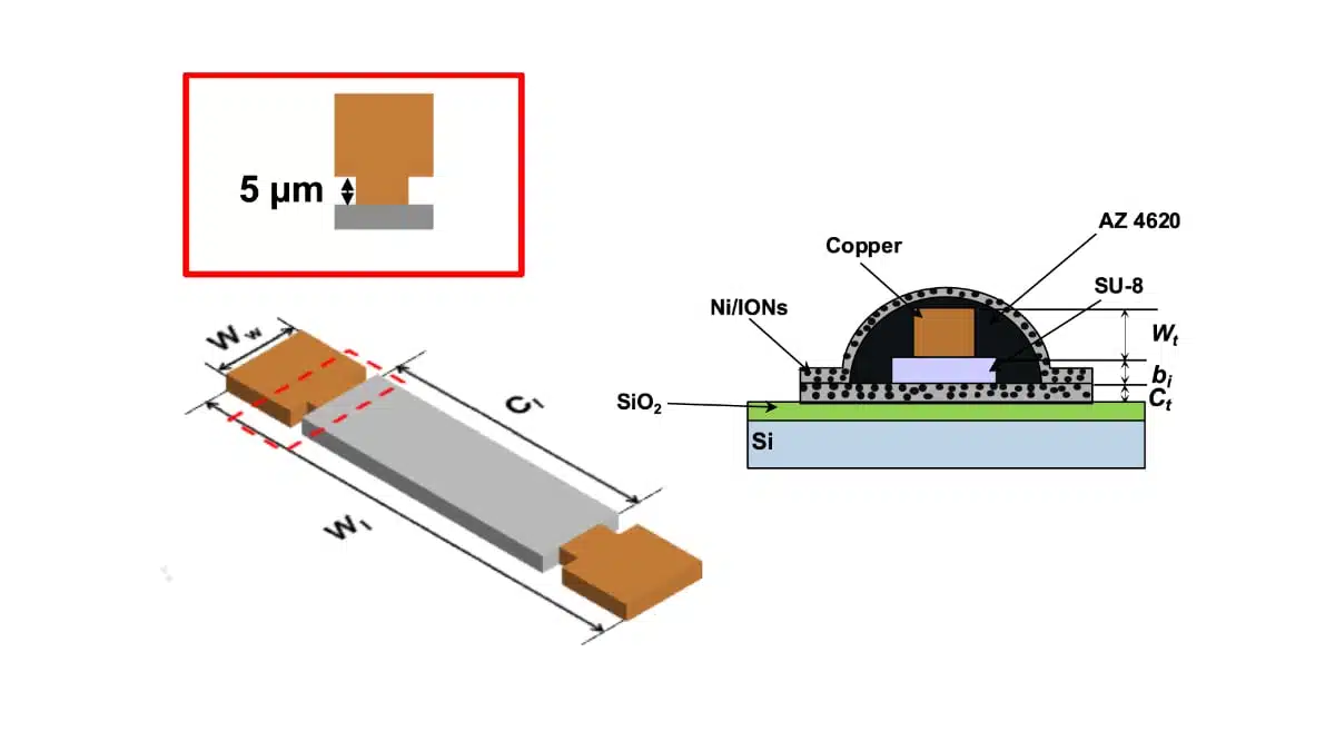
University of Florida researchers have demonstrated stripline microinductors that combine electroplated nickel with iron oxide nanoparticles to increase inductance within a small silicon-based footprint.
Sai Pranesh Amirisetti, Brenden M. Mears, Noah Morgan, Jennifer S. Andrew and David P. Arnold published the peer-reviewed work in the Journal of Micromechanics and Microengineering on 29 September 2026.
Key takeaways
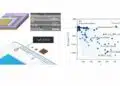
- Devices with approximately 4 µm-thick nickel/iron oxide nanoparticle cores achieved about 1.6 nH in reported areas of 0.01–0.015 mm², with more than twice the inductance of comparable air-core devices.
- Reflowed AZ 4620 insulation enabled approximately 6 µm-thick copper conductors and a peak quality factor of 5.3 at 150 MHz, compared with 3.35 for the earlier SU-8 construction.
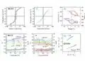
- A separate, co-fabricated bias-test structure maintained approximately 8 nH at 1 MHz over a DC-current sweep from 0 to 330 mA. This is not a current rating for the 1.6 nH devices.
- Wafer testing found 64 functional devices among 97 measured, giving approximately 66% functional yield. The standard-process functional subset had a mean low-frequency inductance of 1.904 nH and standard deviation of 0.083 nH.
Background
Moving power conversion closer to a chip’s load can shorten power-delivery interconnects, but the inductor remains difficult to miniaturize. Increasing switching frequency reduces the inductance required for a given buck-converter voltage and ripple-current target; it also increases the importance of conductor and magnetic losses.
A magnetic core increases flux linkage around a conductor, raising inductance without necessarily adding turns. However, a continuous metallic core can support circulating eddy currents that increase loss and weaken its high-frequency magnetic response. The practical objective is therefore not maximum permeability alone, but a useful balance of permeability, resistivity, saturation margin and winding resistance.
The Core Magnetic Materials, Permeability and Their Losses guide explains these competing requirements at component level.
Earlier approaches cited in the paper include sputtered magnetic multilayers and laminated electroplated cores. Electro-infiltration takes a different route: nickel is plated through a porous nanoparticle template, forming a heterogeneous magnetic composite rather than a homogeneous metal film.
What the researchers found
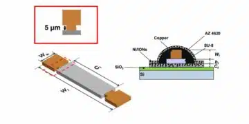
The device encloses an insulated copper strip between bottom and top nickel/iron oxide nanoparticle layers, designated Ni/IONs. This is a nickel-matrix composite containing iron oxide nanoparticles—not a conventional nickel–iron alloy core.
The nanoparticles were synthesized by aqueous precipitation. X-ray diffraction with Rietveld refinement supported a magnetite structural model and yielded a crystallite size of approximately 16.6 nm. Nickel infiltration used a sulfamate electrolyte at 54 °C and 10 mA/cm², with a magnet behind the substrate to retain the particles.
Fabrication combined photolithography, sputtered seed layers, electroplating, planarization and polymer insulation. Surface roughness initially threatened dielectric integrity, making polishing an important integration step.
A second problem emerged above the conductor. SU-8 produced steep sidewalls that hindered continuous upper-core coverage. Limiting copper thickness improved coverage but increased winding resistance. Thermally reflowing AZ 4620 at approximately 200 °C rounded the profile, allowing thicker copper while preserving the magnetic enclosure.
| Parameter | SU-8 construction | AZ 4620 construction | Conditions and interpretation |
|---|---|---|---|
| Copper conductor thickness | Approximately 2 µm | Approximately 6 µm | Fabricated cross-sections; different process variants |
| Peak quality factor | 3.35 | 5.3 | On-wafer small-signal measurements; optimized peak at 150 MHz; SU-8 peak frequency not specified in the accompanying text |
| Peak-Q improvement | Reference | Approximately 58% | Comparison of each variant’s peak, not necessarily an equal-frequency comparison |
| Upper dielectric profile | Steep sidewalls | Rounded after reflow | AZ 4620 treated at approximately 200 °C |
The result illustrates why core material and winding process cannot be optimized independently. The higher quality factor came from the combined effects of thicker copper and improved magnetic-path continuity—not from a change in magnetic composition.
Prior material characterization, summarized in the paper, gave relative permeability of approximately 23 and magnetic loss tangent of approximately 0.10 at 10 MHz. These material-level values must not be substituted for device performance at 150 MHz. The paper also cites a magnetic-loss resonance near 350 MHz, reinforcing the need to distinguish measurable inductance from efficient energy storage.
Device characterization used a calibrated vector network analyzer and on-wafer probes. The wafer study covered 97 inductors, but the reproducibility statistics describe 51 functional standard-process magnetic-core devices, not the entire fabricated population. Measurement temperature and RF excitation level were not specified in the accessible methods text.
Why it matters for passive components
The direct relevance is to integrated power inductors for power supply on chip and power supply in package. The contribution is a fabrication route that increases inductance around a short copper conductor while avoiding high-temperature magnetic annealing.
For stripline microinductors, the useful design relationship is
Increasing inductance helps only if effective AC resistance remains controlled. Here, that resistance includes winding loss, magnetic loss and substrate, dielectric and parasitic contributions. A peak Q of 5.3 is therefore a device-level result, not a converter-efficiency measurement.
The approximately 330 mA bias result also requires careful interpretation. It came from a dedicated one-port structure with different dimensions and approximately 8 nH inductance. It demonstrates stable incremental inductance within that test range, but establishes neither the saturation threshold nor the continuous thermal capability of the smaller devices. These distinctions are central to Power Inductors and Storage Chokes.
For component developers, the opportunity is a thicker magnetic composite deposited by electrochemical processing. For sourcing engineers, it remains a research process rather than an interchangeable catalog technology.
From lab to component: stripline microinductors
An editorial maturity estimate is TRL 4: fabricated devices validated in a laboratory, without demonstration in a complete converter or a representative qualified package.
The authors identify the approximately 200 °C dielectric-reflow step and absence of magnetic annealing as favorable for post-BEOL integration. That is a thermal-budget argument, not proof of foundry compatibility. The demonstrated substrate preparation also includes thermally grown silicon dioxide; integrating the subsequent stack onto finished circuitry would require a compatible starting surface and process sequence.
Manufacturing readiness is constrained by yield. Failures were spatially clustered, and visual inspection suggested film-stack delamination associated with thermal stress during AZ 4620 curing. Slower heating and cooling were proposed as remedies, but improved yield after that change was not demonstrated.
The 1.904 nH mean and 0.083 nH standard deviation indicate approximately 4.4% relative variation among the selected functional devices. They do not establish production tolerance across failed devices, repeated wafers or manufacturing lots.
Additional development must address dielectric lifetime, adhesion, moisture response, temperature-dependent magnetic properties and high-frequency self-heating. Nickel-containing chemistry and hydrofluoric-acid processing also require controlled manufacturing practices; the paper does not establish finished-component environmental compliance or production cost.
What engineers should watch
- Converter-level validation: efficiency, ripple, transient response and EMI with the fabricated inductor, rather than inference from small-signal Q.
- Combined bias and frequency testing: inductance and loss under DC current plus representative switching ripple, including the region around the 150 MHz Q peak.
- Thermal current capability: temperature rise, conductor reliability and safe operating limits for the actual device geometry.
- Process reproducibility: repeated-wafer statistics, defined electrical acceptance criteria and demonstrated reduction of delamination.
- Insulation and package reliability: leakage, breakdown, humidity exposure, thermal cycling and adhesion after packaging.
- Integration economics: nanoparticle deposition uniformity, polishing throughput, contamination controls and total processing cost.
Summary
The study demonstrates that an electro-infiltrated nickel/iron oxide core can increase the inductance of a compact copper stripline, while dielectric-profile engineering enables thicker conductors and a higher peak quality factor.
This remains a laboratory device technology. The central design lesson is that magnetic-material performance, conductor resistance and fabrication geometry must improve together; nominal inductance enhancement alone does not establish a useful power-converter component.
Further reading
- Understanding Inductors With Gapped Cores
- Industry’s First Single-Chip Power Converters with On-Chip Thin-Film Magnetic Power Inductors
Source
This article is based on the peer-reviewed paper published in the Journal of Micromechanics and Microengineering, available as publisher-hosted open access under the Creative Commons Attribution 4.0 license. No matching university or institute press release was located. These are research devices, not qualified commercial components; design decisions should await manufacturer specifications and qualification appropriate to the application.
References
- Sai Pranesh Amirisetti, Brenden M. Mears, Noah Morgan, Jennifer S. Andrew and David P. Arnold, “Stripline microinductors using electroinfiltrated nickel-iron oxide nanocomposites for power supply on chip applications,” Journal of Micromechanics and Microengineering, vol. 36, no. 9, article 095014, 2026. Published 29 September 2026. https://doi.org/10.1088/1361-6439/aea912. CC BY 4.0. Publisher article and PDF consulted.