

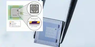




A team led by Prof. Min Hyuk Park at Seoul National University, working with Hanyang University, Pohang Accelerator Laboratory, Chonnam National University and Samsung Electronics, has reported a 5 nm ferroelectric HZO capacitor that switches fully at 0.6 V.
The peer-reviewed paper was published in Nature Communications on 29 October 2026. It shows that engineering the titanium nitride electrode, not changing the ferroelectric itself, can lower switching voltage while keeping both speed and cycle life.
Key takeaways
- A 5 nm Hf0.5Zr0.5O2 (HZO) capacitor on a (111)-textured TiN bottom electrode reaches saturated switching at 0.6 V: 2Pr = 31.5 µC/cm², Ec = 0.62 MV/cm, Vc ≈ 0.31 V (100 µm², 1 kHz).
- Measured 50% switching time on a 25 µm² device is 42.1 ns at 0.6 V and 8.1 ns at 1.0 V. Extrapolation to a (250 nm)² footprint gives sub-ns to low-ns switching.
- No hard breakdown occurred through 10¹² bipolar cycles at 0.6–1.0 V. With a fatigue-loss criterion below 20%, endurance is 6 × 10¹¹ cycles at 0.6 V and 10¹² cycles at 1.0 V.
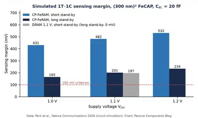
- In circuit simulation of a common-plate 1T–1C memory cell at 1.1 V, the capacitor keeps a 201 mV long stand-by sensing margin, where a dielectric DRAM cell drops to 0 mV.
Background: ferroelectric HZO capacitor scaling
Ferroelectric hafnium zirconium oxide is the thin-film ferroelectric that the semiconductor industry can actually use. It is CMOS-compatible, grown by atomic layer deposition (ALD) and keeps its ferroelectricity below 10 nm. Besides the linear dielectric charge, switching its polarization adds a non-volatile charge of about 2Pr. For a 5 nm film at 1.2 V, the dielectric part is about 6.4 µC/cm², while 2Pr is 30–60 µC/cm². That is a 5–10× gain in storable charge per area, the parameter that limits DRAM capacitor scaling.
Two physical limits stand in the way. First, the coercive field rises as the film gets thinner, following the Kay–Dunn relation:
Thinner films therefore do not reduce the switching voltage as much as expected. Second, faster switching normally needs a higher field, and higher fields shorten endurance. In ultrathin stacks, both problems are made worse by voltage lost across a parasitic oxide layer at the electrode interface. Readers who follow ultra-thin ferroelectric capacitors for compact memory will recognize this as the main barrier to sub-volt operation.
What the researchers found
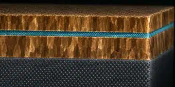
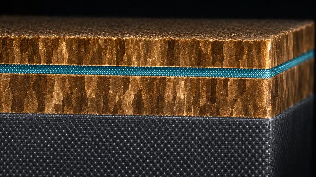
The team deposited the TiN bottom electrode by plasma-enhanced ALD. Using NH3/Ar plasma instead of N2/Ar produces a (111)-textured TiN with a nitrogen-rich, oxidation-resistant surface. On the bare electrode, the fitted TiO2 contribution is about half that of (002)-textured TiN. After HZO growth, the bottom interfacial layer is thinner and more uniform: 0.5 ± 0.2 nm versus 0.7 ± 0.4 nm. The HZO grains are also more strongly oriented, and nitrogen does not diffuse noticeably into the HZO.
A direct comparison on large 40,000 µm² capacitors shows the electrical effect of the electrode texture.
| Parameter | HZO on TiN-(111) | HZO on TiN-(002) |
|---|---|---|
| Saturation voltage | 0.8 V | 1.2 V |
| 2Pr at saturation | 31.8 µC/cm² | 26.5 µC/cm² |
| Ec at saturation | 0.70 MV/cm | 0.94 MV/cm |
| Intrinsic Vc (extrapolated) | ≈ 0.28–0.29 V | ≈ 0.42–0.44 V |
| Vc variation, 30 devices (0.8–1.4 V) | 1.4–1.9% | 2.1–3.2% |
| NLS median switching time t1 at 1.0 V | 3.89 µs | 8.60 µs |
Table note: 5 nm Hf0.5Zr0.5O2 MFM capacitors, 40,000 µm²; each stack is compared at its own saturation condition. Intrinsic Vc is extracted after removing rate- and series-resistance effects.
On patterned 100 µm² devices, the optimized stack switches completely at a 0.6 V amplitude, and the switching current peaks lie fully inside the voltage window. 2Pr rises to 37.3 µC/cm² at 1.0 V, while Ec stays within 0.54–0.68 MV/cm.
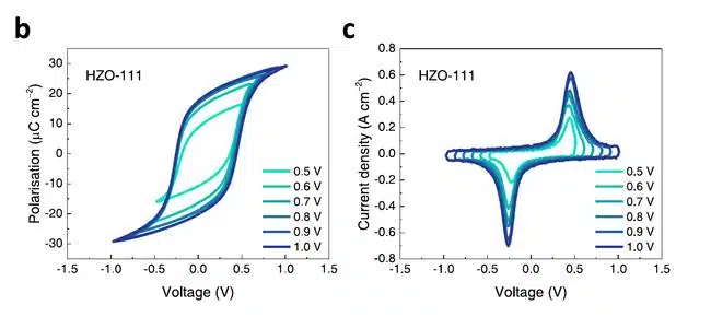
The measured coercive fields lie below the Kay–Dunn trend line for ultrathin HfO2-based films. The authors explain this with finite screening in the electrodes. Before reversal, the depolarization field points the same way as the applied switching field and helps it. After correcting for this effect, the thickness exponent comes back to −0.63 ± 0.03, close to −2/3. In other words, the Kay–Dunn law still holds; what improves is the external voltage needed in practice.
Switching speed depends on capacitor area. Across devices from 40,000 µm² down to 25 µm², the 50% switching time falls steadily, because smaller capacitors contain fewer slow-switching grains. The activation field stays at about 1.1 MV/cm. The Hf:Zr ratio was also varied: 5:5 gave the best balance of polarization, speed and endurance, while Zr-rich films lowered the apparent Ec by moving towards a field-induced transition with less usable charge.
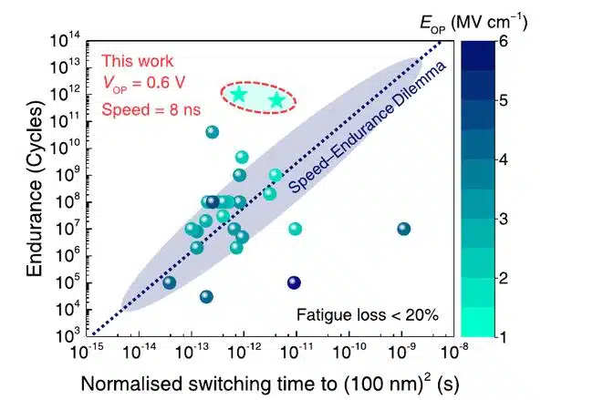
Fatigue increases with cycling voltage. In repeated 10¹¹-cycle steps, the average polarization loss was 11.81% at 1.0 V, 16.63% at 1.5 V and 31.54% at 2.0 V. A 1.6 V rejuvenation treatment recovers much of the lost 2Pr.
At circuit level, the team proposes a common-plate FeRAM (CP-FeRAM). It uses a DRAM-like one-transistor, one-capacitor cell with a fixed DC plate voltage. Simulations with a Verilog-A compact model calibrated to the measured loops give short/long stand-by sensing margins of 431/165, 482/201 and 532/234 mV at 1.0, 1.1 and 1.2 V. These values are for a (300 nm)² capacitor and a 20 fF bit line. For a 200 mV long stand-by target, the minimum capacitor footprint shrinks from (375 nm)² at Pr = 8 µC/cm² to (142 nm)² at Pr = 18 µC/cm². A fabricated 1 × 15 common-plate capacitor array showed 2Pr = 39.09 ± 0.76 µC/cm² after conditioning. Neighbouring cells showed no measurable disturbance over 10¹⁰ aggressor cycles.
Why it matters for passive components
This work concerns embedded capacitors rather than discrete parts, but the physics matches what capacitor engineers deal with every day. The key result is that the electrode/dielectric interface sets the effective field in an ultrathin dielectric. A sub-nanometre oxide layer at the electrode acts as a series capacitance. It takes voltage away from the functional layer and spreads the switching thresholds across devices. The same series-interface effect limits capacitance density in thin-film integrated passive devices and silicon MIM capacitors that use HfO2- and ZrO2-based dielectrics.
For memory capacitors, the trade-off moves from geometry to charge. A higher stable remanent polarization allows a smaller capacitor for the same sense-amplifier margin, so capacitor area can shrink without the deep-trench or tall-cylinder structures that DRAM uses today. The paper also shows that a low coercive field is useful only if it comes with high 2Pr and a narrow switching distribution. A lower Ec bought by moving towards a field-induced phase transition loses usable charge. The same balance applies to the optimal thickness of ferroelectric capacitors and to related antiferroelectric hafnia films for energy storage.
From lab to component
The results come from metal–ferroelectric–metal test capacitors of 25–40,000 µm² and a 15-capacitor array without access transistors. The sub-ns switching at DRAM-scale footprints is an extrapolation from these sizes, not a measurement. The CP-FeRAM sensing margins are circuit simulations, and the array was preconditioned at 1.6 V for 10⁷ cycles before testing. The authors state that transistor leakage, word-line coupling and lifetime prediction still need separate assessment. Editorial estimate: TRL 3–4 for the electrode-engineered capacitor, and TRL 2–3 for the CP-FeRAM concept.
On the positive side, the process is industry-compatible: ALD and PEALD at 250 °C, TiN electrodes and 6-inch wafers with 0.91% resistivity non-uniformity. Samsung Electronics took part as co-author and part-funder. Retention data and temperature-dependent behaviour are not yet reported, and the work depends on a wake-up treatment before operation.
What engineers should watch
- Directly measured switching in nanoscale capacitors at (250 nm)² or smaller, confirming or correcting the area extrapolation.
- Retention and imprint at elevated temperature, which are critical for any non-volatile or refresh-reduced memory claim.
- Full 1T–1C array results with access transistors, including disturbance of half-selected cells and read/write-back energy.
- Wake-up and rejuvenation behaviour in product-like operation, and whether the pre-conditioning step can be removed.
- Transfer of the (111)-TiN interface process to 3D capacitor geometries, which are needed for high-density DRAM.
- Use of the same interface approach in high-density silicon and MIM capacitors that use HfO2/ZrO2 dielectrics.
Summary
The study shows that controlling the texture and surface chemistry of the TiN electrode lets a 5 nm ferroelectric HZO capacitor switch fully at 0.6 V, reach nanosecond-range switching and survive 10¹² cycles without hard breakdown. The common-plate memory concept built on it is supported by simulation and a small capacitor array, so the work is at an early laboratory stage. The key takeaway for designers is that in ultrathin capacitor dielectrics, the electrode interface is as important a design variable as the dielectric itself.
Further reading
- High-Precision Hyperdimensional Computing with Multi-Level Ferroelectric HZO Capacitors
- Imec Demonstrates Capacitor-less IGZO-Based DRAM Cell With >400s Retention Time
Source
This article is based on the peer-reviewed paper published in Nature Communications (Article in Press, open access under CC BY 4.0) and on the accompanying press release from Seoul National University. These are research results on test structures, not qualified commercial components. Engineers should wait for manufacturer data and standard qualification before making any design decision.
References
- G. H. Park, S. Jo, S. Park, Y. H. Cho, H. S. Choi, H. W. Jeong, S. H. Kim, D. H. Lee, M. Jeong, T. Kwon, D. H. Kim, G. Y. Lee, S. Jeong, Y. Y. Kim, S. Y. Lee, Y. Lee, J. Park, C. H. Jung, H. Lim, D. Kwon, H. J. Kim, M. H. Park, “Resolving the Kay–Dunn limit and the speed–endurance dilemma in ferroelectric Hf0.5Zr0.5O2 for DRAM-class sub-volt capacitors,” Nature Communications, 2026, https://doi.org/10.1038/s41467-026-78705-4, CC BY 4.0
- Seoul National University, press release on the low-voltage, high-endurance HZO capacitor, published via Tech Xplore, 4 November 2026, https://techxplore.com/news/2026-11-voltage-capacitor-combines-rapid-trillion.html