





source: EDN article
Thomas Kugelstadt, Intersil Corporation -August 23, 2016 explains passive fail safe biasing by resistor networks in RS-485 systems in his EDN article.
With RS-485 networks, there are periods of time when no driver is actively driving the bus, such as when one driver relinquishes the bus to another driver. During this time, the termination resistors collapse the differential bus voltage to 0V, which is an undefined input level for many RS-485 receivers. Faced with this undefined input, a receiver might output the wrong logic state or worse yet, it might oscillate. The oscillation may be interpreted as an endless stream of message start bits, causing the controller to waste valuable bandwidth trying to service these phantom messages. Fail-safe bus biasing is one way to alleviate this problem.
Passive fail-safe biasing is accomplished through resistor networks of pull-up, termination, and pull-down resistors whose voltage divider action provide a differential dc bus voltage, VAB, when no driver is actively driving the bus (see Figure 1).

Figure 1: Passive fail-safe biasing network for short to medium bus distance
To drive all receiver outputs to the defined idle state of a logic high, VAB must be higher than the maximum input threshold, VIT-MAX. In addition, sufficient noise margin should be added to allow for operation in harsh industrial environments, thus making VAB = VIT-MAX + VNoise.
This article helps system engineers design successful fail-safe biasing networks by providing equations for calculating the resistor values and the maximum possible bus loading caused by transceivers for single and dual fail-safe terminations. We also present the ISL315x family of high VOD transceivers, whose common-mode 60 unit loads (ULs) drive capability far exceeds the 32 ULs of standard transceivers.
Single Fail-safe Biasing Network Design
For short network distances of ≤ 100m and low- to medium-idle bus voltages of 0.05V ≤ VAB ≤ 0.3V, fail-safe biasing at one bus end will often suffice. For simplification, the network shown in Figure 1 is converted into the lumped equivalent circuit of Figure 2. Note the bias resistors, RB, and the termination resistors, RT1, and RT2. REQ representing the equivalent input resistance of all transceivers connected to the bus.

Figure 2: Lumped equivalent model of Figure 1 circuit
Prior to deriving the equations for calculating the resistor values, we establish the conditions that must be satisfied for line termination and common-mode loading.
1) The cable end without the biasing network is terminated with RT1, whose value should match the characteristic impedance of the cable, Z0.

2) For line impedance matching during normal operation, the series combination of the two biasing resistors in parallel with the termination resistor, RT2, must match the characteristic cable impedance: Z0 = 2RB||RT2. Thus, for a given value of RB, RT2 becomes:

3) RS-485 specifies the maximum common-mode load, which a standard compliant transceiver must be able to drive with 32 parallel ULs. One unit load represents a minimum common-mode resistance of around 12kΩ between each signal conductor and ground. Thus, the total common-mode loading of 32 ULs results in a minimum common-mode resistance of RCM = 375Ω.
Because the bias resistors present a common-mode load in addition to the equivalent transceiver input resistance, the parallel combination of RB and REQ must be greater or equal to RCM: RB||REQ ≥ RCM. For a given RB value, REQ is therefore limited to:

To find the equation for calculating RB, we determine the node currents of A and B in Figure 2, and solve for the individual line voltages, VA and VB.

Then calculating the difference between the line voltages provides the differential bus voltage:

Inserting EQs. 1, 2 and 3 into EQ. 4 provides the final equation for the dc-bus idle voltage:

And solving for RB yields the minimum required bias resistor value:

Common-Mode Loading
Because passive fail-safe biasing presents additional common-mode loading, it is necessary to determine the maximum number of transceiver unit loads, nUL, that can load the bus without dropping below RCM = 375Ω.
nUL is the ratio of the common-mode resistance of one unit load to the common-mode resistance of the transceiver unit load: nUL = 12kΩ / REQ, and inserting EQ. 3 for REQ yields:

This maximum number of transceiver unit loads can be accomplished using n x 1UL, 2n x 1/2UL, 4n x 1/4UL, or 8n x 1/8UL transceivers.
Dual Fail-safe Biasing
To maintain a constant VAB over long cable lengths, fail-safe biasing at both bus ends is necessary. Each biasing network compensates for the loss of biasing the other network along the cable run.
Figure 3 shows the lumped equivalent circuit of a bus with dual fail-safe biasing.

Figure 3: Lumped equivalent model for dual fail-safe biasing
The requirements for the termination resistors, RT, are the same as for RT2 in the single fail-safe biasing network demanding that Z0 = 2RB||RT. Hence, for a given RB, RT must be:

However, the condition for common-mode loading changes because each conductor now sees two biasing resistors in parallel to ground. Thus, the parallel combination of RB/2 and REQ needs to be greater or equal to RCM: RB/2 || REQ ≥ RCM. Hence, for a given RB value, REQ is limited to:

To find the equation for RB, we determine the node currents into A and B. Because the biasing networks are identical, they drive the same amount of current through REQ. Therefore, we have to establish only one current through REQ and multiply it by a factor of two to determine VAB in the middle of the bus.

Solving the node currents for the individual line voltages, VA and VB, and calculating the difference between them provides the differential bus voltage:

Inserting EQs. 8 and 9 into EQ. 10 provides the final equation for VAB:

And solving for RB yields the minimum required bias resistor value:

With RB in place, the maximum number of transceiver unit loads can now be calculated via:

Note, because the RB value for dual failsafe biasing is twice the RB value for single fail-safe biasing, nUL remains the same for both applications.
Calculation Examples
In the following examples, we calculate the resistor values for the single and dual fail-safe biasing networks of a short and a long data link assuming a characteristic impedance of Z0 = 120Ω. The ISL8487E bus transceiver is used in this example. This device is a 1/8 UL transceiver with a minimum supply of Vs = 4.75V. Its maximum receiver input threshold is 200mV which, assuming a 100mV noise margin, requires an idle bus voltage of VAB = 300mV.

Transceiver Selection
Selecting the best transceiver to address noise immunity and output drive capability is important for robust network design for two reasons.
- During times when the bus is not actively driven, there should be sufficient noise margin to prevent a receiver from false triggering, even in very noisy environments.
- During normal data transmission, the active driver must be able to drive the added common-mode load created by fail-safe biasing and still provide a signal with sufficient noise margin to remote transceivers.
For example, the first-generation ISL8487E device has a positive receiver input threshold of VIT-max = 200mV. Adding just a small noise margin of 50mV makes VAB = 200mV + 50mV = 250mV.
Compare this to a second-generation transceiver, such as the ISL83082E with full fail-safe capability. Its receiver output turns high whether the receiver inputs are floating (bus open) or shorted (bus short or idle).
Full fail-safe capability is accomplished by offsetting the maximum input threshold to a slightly negative level, in this case -50mV. To provide the same 50 mV noise margin, a VAB of 0V is sufficient for eliminating the need for external fail-safe biasing. Without a biasing network, all 32 unit loads are available to the bus transceivers.
In modern industrial applications with high electrical noise pollution, industrial networks, such as PROFIBUS, use dual fail-safe biasing with idle bus voltages of 0.6V and more. VAB levels that high require the bias resistors to be of such low resistance that their combined value drops far below the minimum common-mode resistance of 375Ω. When this happens, the calculation of nUL will result in negative values. In fact, it is possible to calculate the maximum VAB (when nUL = 0) by making RB/2 = RCM in EQ. 12 and solving for VAB:

Hence, networks requiring high VAB levels need dedicated transceivers that provide much higher differential and common-mode drive capability than standard compliant transceivers.
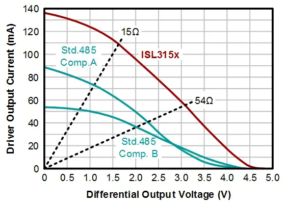
One transceiver series able to meet these demands is Intersil’s ISL315x family of large VOD transceivers. These devices are capable of driving up to eight 120Ω terminations in parallel at a minimum differential output of VOD-MIN = 1.5V, (see Figure 4) and more than 60 dc-unit loads over a common-mode voltage range from -7V to +12V at a minimum VOD of 2.4V (see Figure 5).

Figure 4: Differential output drive capability, ISL315x vs standard RS-485 transceivers

Figure 5: Common-mode output drive capability, ISL315x vs standard RS-485 transceivers
The ISL315x’s superior output drive capability provides enhanced noise immunity even to the most remote bus transceiver, while enabling twice the common-mode loading compared to standard RS-485 transceivers.
Table 1 lists the resistor values for single and dual fail-safe biasing networks and compares the available transceiver unit loads for two standard transceivers, ISL8487 and ISL83082, and the high-VOD transceiver, ISL3152, as a function of noise margin.
Table 1. Resistor values and unit loads for standard and high VOD transceivers as a function of noise margin

Transceivers with 200mV input threshold, such as the ISL8487, only allow for low idle-bus noise margins of up to 100mV. Beyond that, the required rise in VAB demands the bias resistor values to be so low that the resulting numbers in transceiver unit loads turns negative.
Full fail-safe transceivers, such as the ISL83082, require much lower VAB values due to their negative input threshold of -50mV. This allows for much higher bias resistor values and consequently higher numbers of required bus transceivers. Both transceiver types however have standard drive capability of up to 32 unit loads, which limits their use in noisy environments to networks with standard noise margins and low transceiver counts.
In strong contrast, the ISL3152, with its high VOD, easily drives more than twice the transceiver count at medium noise levels and still manages to support up to 100 transceivers at 600mV noise margin. To accomplish even higher noise margins, an increase in the characteristic cable impedance is necessary. This is done in PROFIBUS where Z0 = 150Ω, thus necessitating higher values for RT and RB to lower common-mode loading of the biasing networks.
Conclusion
Creating a fail-safe biasing network ensures stable network node operation during periods of time when the bus is not actively driven. In addition, the common-mode loading caused by the bias resistors must be driven by an active driver during normal data transmission. The high noise margins required in industrial networks demand low bias resistor values whose common-mode load can overburden the drive capability of standard RS-485 transceivers. This problem can be alleviated with the ISL315x family of large output voltage-swing transceivers, capable of driving up to eight 120Ω terminations and more than 60 dc-unit loads. In combination with the equations provided in this article, these transceivers ease and accelerate the design of fail-safe biasing networks.