binder is introducing printed electronics directly on three‑dimensional connector and device components, allowing sensors, heaters and conductor tracks to be integrated into the surface rather than added as separate assemblies.
This approach targets compact, decentralized automation and IIoT designs where installation space, reliability and integration effort are critical.
Key features and benefits
- Functional layers printed directly on the component surface
Sensors, heating elements and conductor tracks are printed onto the outer or inner surfaces of components, turning housings and connector bodies into functional elements rather than passive mechanics. - Support for plastic, metal, glass and ceramic substrates
The process at the binder Innovation and Technology Center (ITZ) supports a wide range of engineering materials, enabling integration into connector housings, mechanical parts and device enclosures. - Screen and pad printing with conductive and dielectric pastes
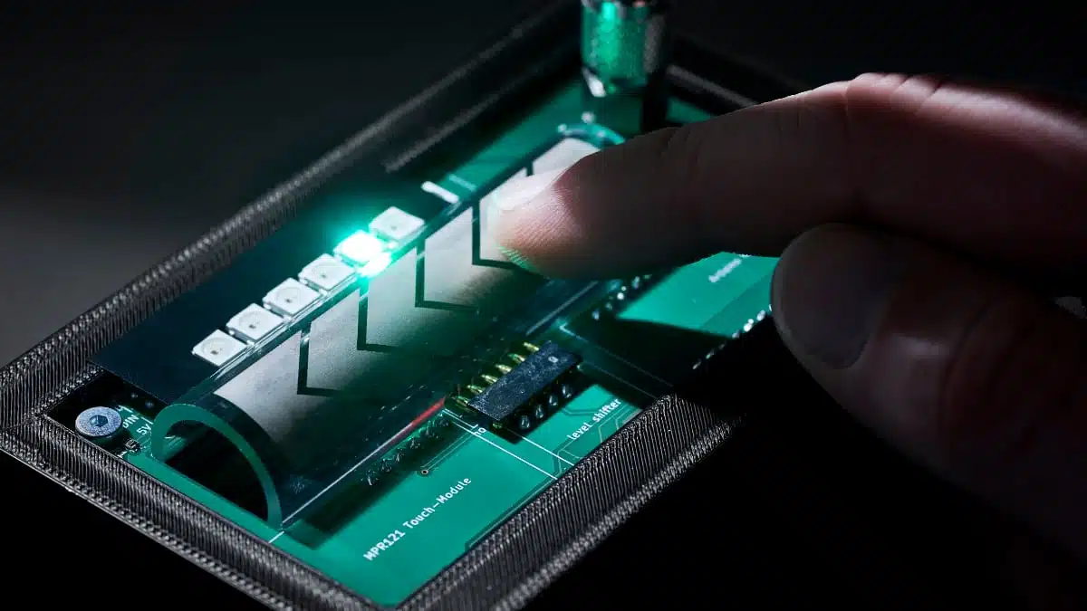
High‑precision screen and pad printing techniques are used with conductive pastes based on silver, copper, carbon or PEDOT:PSS, combined with dielectric layers to form defined functional stacks. - Multilayer structures on 3D and curved surfaces
Multilayer printing enables routing of conductor tracks and implementation of sensors or heaters even on complex 3D geometries where conventional rigid or even flexible PCBs become difficult to accommodate. - Reduction of individual parts and assembly steps
By moving function onto the surface, separate PCBs, wire harnesses, and sensor modules can be eliminated, reducing mechanical interfaces, connectors and mounting hardware. - Lower weight and more compact designs
Integrating function into the component shell reduces overall mass and enables slimmer device designs, which is particularly relevant in mobile machinery, robotics and compact automation nodes. - Higher reliability through fewer interconnects
Each omitted plug connection, solder joint or separate sensor reduces potential failure points; printed structures can be designed as part of the overall connector system for better robustness over life. - Short path from prototype to series solution
The ITZ develops and validates printed electronics processes and prototypes, while binder solutions adapts them to customer‑specific series production, keeping one supply chain from concept to series component.
Typical applications
Printed electronics on connector and device surfaces is especially relevant wherever functions must be packed tightly in harsh or mechanically constrained environments.
- Mechanical engineering and industrial automation
- Condition monitoring sensors (temperature, strain, vibration–related sensing concepts) integrated on housings or connector shells for predictive maintenance.
- Local heating elements to prevent condensation or ensure stable operating temperatures in cabinets, sensors or actuators.
- Operator interfaces and HMI components
- Printed touch and force sensors on front panels or connector‑adjacent surfaces as replacements for mechanical buttons and switches.
- Customizable HMI geometries, where the sensing pattern follows a curved or ergonomic surface.
- Energy and renewables
- Printed temperature or current‑related sensing structures on connectors and busbar interfaces in inverters, string combiners or junction boxes.
- Integrated heating or sensing around sealing areas to ensure tightness and safe operation under varying climates.
- Transport and heavy machinery
- Functionalized connectors with integrated sensors on curved housings in vehicles, construction machinery or agricultural equipment.
- Weight‑sensitive applications where replacing secondary PCBs and mounting hardware yields tangible mass reduction.
- Medical and test equipment
- Compact, sensor‑rich connectors and adapter modules where hygiene, ease of cleaning and minimal protrusions are important.
- Printed tracks and heaters on instrument surfaces where conventional board placement is mechanically impractical.
Example integration scenarios
- A circular connector whose rear shell carries printed temperature sensors and a heater ring to keep sealing areas above dew‑point in outdoor automation nodes.
- A machine tool sensor module where strain‑sensing patterns are printed directly on a curved metal housing to detect load or vibration without additional sensor packages.
Technical highlights
At the heart of this solution is the ability to print electrically functional layers directly on ready‑formed parts rather than on flat substrates.
Printing technologies and materials
- High‑precision screen printing for structured, repeated patterns on accessible surfaces.
- Pad printing for transferring functional structures onto curved or more complex geometries.
- Conductive pastes based on:
- Silver
- Copper
- Carbon
- PEDOT:PSS (a conductive polymer system often used for transparent or flexible applications)
- Dielectric pastes used as insulating layers or to build multilayer stacks with defined creepage and clearance paths.
Functional elements
- Conductor tracks
Printed traces can replace internal wiring or small PCBs, routing signals and power along the component surface. In practice, this allows One Cable concepts and smart connector shells where only a minimum of discrete wiring is left inside the housing. - Sensors
By shaping the printed pattern and material stack, the same process can implement different sensor types, for example:- Temperature sensors using resistive structures
- Force or pressure‑sensitive surfaces for HMI applications
- Other sensor principles according to customer design
- Heating elements
Resistive heating structures can be printed along specific areas to:- Maintain minimum temperature in cold environments
- Avoid ice or condensation formation on connectors and exposed surfaces
- Keep sensors within their intended operating range
Printed electronics concept overview
| Aspect | Printed electronics on components |
|---|---|
| Substrates | Plastic, metal, glass, ceramic |
| Printing methods | Screen printing, pad printing |
| Conductive materials | Silver, copper, carbon, PEDOT:PSS |
| Additional layers | Dielectric pastes for insulation and multilayer structures |
| Typical functions | Conductor tracks, sensors, heating elements |
| Surface types supported | Flat, 3D‑shaped and curved surfaces |
In engineering terms, this approach moves part of the functional circuit from discrete boards onto the mechanical envelope, so the housing itself becomes an active element in the system design.
Availability and implementation path
The printed electronics offering is not a single off‑the‑shelf component series but a technology platform delivered as part of binder’s connector and custom solution portfolio.
- The binder Innovation and Technology Center (ITZ) in Bad Rappenau develops the printing processes, validates materials and implements functional prototypes.
- binder solutions takes these prototypes and adapts them to customer‑specific geometries, assemblies and production volumes.
- Thanks to vertically integrated capabilities (cable assembly, precision‑turned parts, zinc die‑casting, galvanics and final assembly), the printed structures can be combined with:
- Circular connectors from binder’s standard programs
- Custom connector bodies and housings
- Application‑specific cable and connection hardware
For design and procurement teams, this means the printed electronics are supplied as part of a coordinated overall connector or device system rather than as a standalone printed foil or board.
Design‑in notes for engineers
For engineers familiar with standard connectors and PCBs, printed electronics on 3D surfaces introduces new degrees of freedom as well as new constraints. The following points can help during concept and design‑in phases.
- Think in surfaces instead of boards
- Identify housings and connector shells where surface area is available for printed structures.
- Consider which existing PCBs or wiring harness segments could be replaced by printed tracks.
- Define functions early in the mechanical design
- Because functions are printed onto the component, mechanical geometry and functional layout must be coordinated early in CAD.
- Functional areas (sensor zones, heater zones, conductor paths) should be defined as part of the enclosure design.
- Clarify environmental and electrical requirements
- Specify temperature ranges, humidity, mechanical stress and required lifetime so that suitable conductive and dielectric pastes can be selected.
- Define voltage levels, creepage and clearance requirements for the printed structures, especially when carrying mains or higher DC voltages.
- Consider maintainability and diagnostics
- Plan test pads, measurement points or self‑test routines for printed sensors and heaters.
- Ensure that fault conditions (open circuits, degraded resistance, etc.) can be detected by the system.
- Account for integration with connection technology
- Printed conductor tracks typically interface with crimp contacts, soldered terminations or overmolded interconnects inside the connector body.
- Coordinate interfaces and transition zones together with binder’s engineering team to maintain mechanical and electrical robustness.
- Leverage predictive maintenance architectures
- When designing printed sensors into critical nodes, integrate their outputs into existing condition monitoring and predictive maintenance systems.
- Use the possibility of distributed, surface‑mounted sensing to increase observability of connector temperature, mechanical stress or environmental impact.
- Engage early with binder’s R&D and solutions teams
- Since this is a customer‑specific technology, early dialogue with binder ITZ and binder solutions is essential to align concept, manufacturability and validation effort.
For purchasing and sourcing, it is important to treat such printed‑electronics‑enabled components as part of a coordinated connector solution with defined lifecycle and qualification path rather than as commodity connectors.
Source
This article is based on information provided in an official binder press release and accompanying materials from the binder Innovation and Technology Center, interpreted and contextualized for design engineers and procurement professionals.