



This article explains how decomposing switching waveforms into harmonics can support the design of inductors, capacitors, gate drivers, and EMI mitigation. It is based on expanded and edited application note “Calculating Current Induced by Square-Wave Voltages in Power Electronics Circuits,” authored by Jake Michels of the YAGEO Group.
Key Takeaways
- Square-wave harmonics influence RMS currents in power converters, affecting component stress and electromagnetic interference.
- This article provides a method to calculate currents from square-wave voltages using Fourier decomposition for better design decisions.
- Inductors mostly handle lower-order harmonics, while capacitors like MLCCs face stress from high-order harmonics.
- The design implications for various components depend on harmonic content, which must inform current ratings and thermal management.
- A practical workflow exists to estimate RMS currents based on square-wave harmonics, aiding in component sizing and verification.
Introduction
Square-wave voltages are ubiquitous in switched-mode power supplies, appearing at MOSFET gates, switching nodes, rectifiers, clamps, and PWM control interfaces. Unlike DC or pure sinusoidal excitation, square waves contain substantial high-frequency harmonic content that materially affects RMS currents, component stress, EMI, and reliability.
This article outlines a practical method for estimating currents induced by square-wave voltages using Fourier harmonic decomposition, then connects the results to design decisions for inductors, capacitors (especially MLCCs), MOSFET gate drivers, and EMI filters. It complements the topology-level discussions in your articles on buck and boost converters (buck converter design and calculation, boost converter design and calculation) and resonant and isolated converters (LLC resonant converter design and calculation, flyback converter design and calculation, SEPIC converter design and calculation), as well as the broader system view in the power converter dossier.
Square waves in practical converters
Square-wave signals arise in virtually all PWM-based and many resonant power stages, including: MOSFET gate drive waveforms, switching-node voltages in synchronous buck and boost converters, controller outputs, and rectifier/clamp node waveforms. The SW-node waveforms discussed in buck converter design and calculation and boost converter design and calculation guides are classic examples of near-square switching voltages in hard-switched topologies.
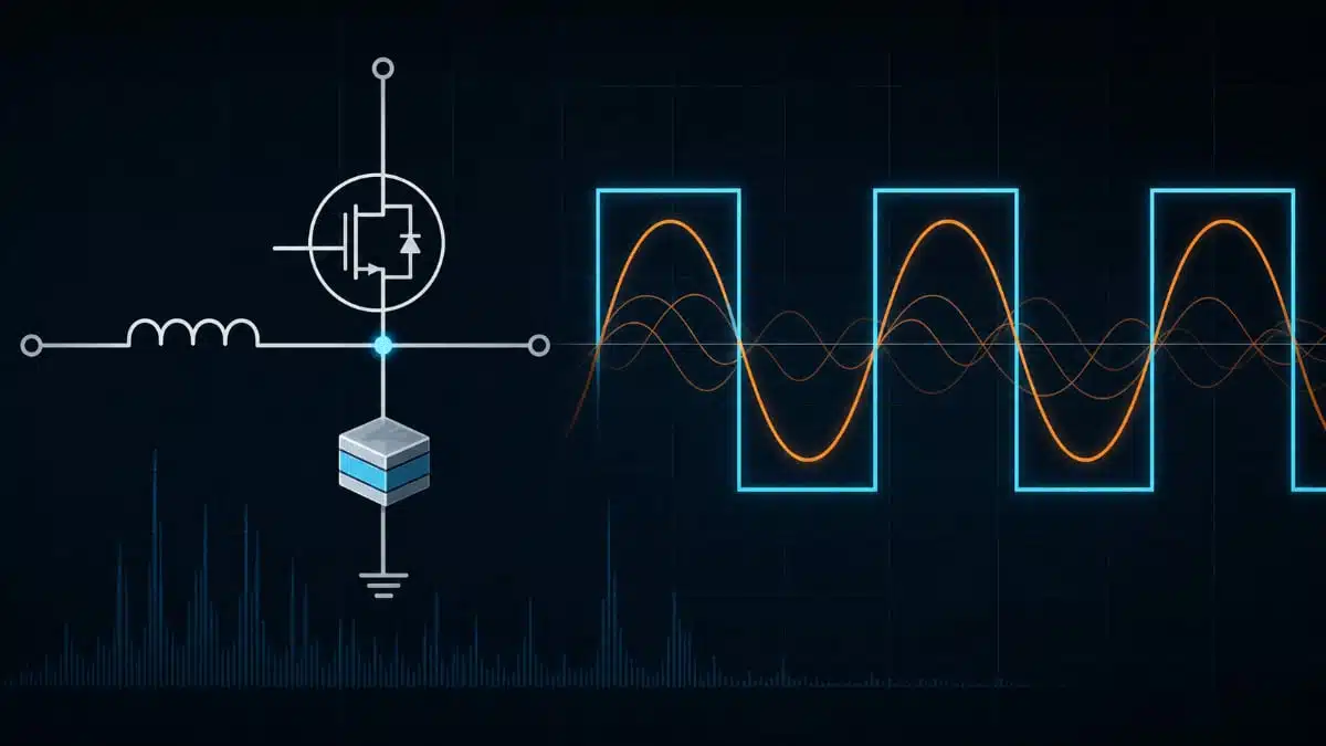
Their non-sinusoidal nature means they cannot be fully described by a single frequency; instead, they consist of a fundamental at the switching frequency plus odd harmonics extending well above the converter’s nominal bandwidth. In resonant and isolated designs such as the LLC resonant converter, flyback converter, and SEPIC converter, the fundamental is shaped by the magnetics and tank, but gate and drive signals still generate harmonic content that couples into the power stage and EMI structure.
Fourier decomposition of switching waveforms
Any periodic waveform can be expressed as a sum of sinusoidal components at integer multiples of the fundamental frequency. For a symmetric square wave with peak amplitude V and switching angular frequency , the voltage can be written as:
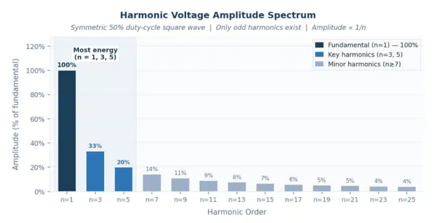
Only odd harmonics are present in this case, and the amplitude of the nth harmonic decreases approximately as 1/n, so higher-order components fall off with harmonic order. This spectral viewpoint ties directly into the small-signal and frequency-domain analyses, where impedance and gain vary strongly with frequency.
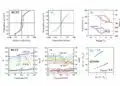
For a symmetrical square wave with peak amplitude V, the harmonic amplitudes decrease as 1/n, so higher-order components fall off with harmonic order, as illustrated in Figure 1. below.
General method for current calculation
Because impedance depends on frequency, current must be evaluated separately for each harmonic component of the square wave. A practical workflow for design and verification is:
- Decompose the relevant square-wave voltage into harmonic components using the Fourier series.
- Determine the circuit impedance at each harmonic frequency nω for the path of interest (inductor, capacitor, gate, EMI network).
- Compute the current amplitude for each harmonic using .
- Combine the harmonic currents via RMS summation to obtain total RMS current: , where N is chosen based on system bandwidth.
This fits naturally with the SPICE/FFT-based workflows you use in your converter design and calculation series and provides a clear bridge between time-domain waveforms and frequency-domain component stress.
Inductor current from switching-node square waves
In hard-switched buck and boost converters, the power inductor is often directly connected to a switching node carrying a square-like voltage waveform. For an inductor, the impedance increases linearly with frequency according to , so substituting this into the harmonic analysis yields current that drops rapidly with harmonic order.
Inductors therefore naturally attenuate higher harmonics, and the fundamental component dominates RMS current in inductive paths, with more than 98.5% of RMS current often carried by the first harmonic in typical cases. This aligns with the current waveforms and copper-loss discussions in your inductor sizing sections within the buck and boost converter design articles.
Capacitor ripple current and MLCC stress
Capacitors behave in the opposite manner: their impedance magnitude decreases with frequency, , so harmonic current scales with frequency for a given harmonic voltage. As a result, high-order harmonics can significantly increase RMS current through MLCCs, DC-link capacitors, and snubber or clamp capacitors, even when average voltage appears modest.
This directly reinforces the MLCC selection and derating guidelines, where ripple current, self-heating, and resonances are critical. The key takeaway is that capacitor stress is dominated by fast edges and high-frequency content at the switching node, not just low-frequency output ripple.
Gate-drive currents in hard-switched stages
Gate drivers apply a square-wave voltage to a largely capacitive MOSFET gate, so gate current is determined by the charge and discharge of this capacitance as . Fast rise and fall times dramatically increase peak gate current demand, especially in high-power buck, boost, flyback, and SEPIC stages where large FETs are used.
In this context, the same harmonic content that affects MLCC ripple also determines the instantaneous loading on gate drivers and associated supply rails.
RMS current estimation and bandwidth limits
Summing an infinite harmonic series is neither necessary nor practical. In design work, engineers typically limit the harmonic count to an order corresponding to the effective bandwidth set by rise/fall times and the parasitics of the power stage and layout.
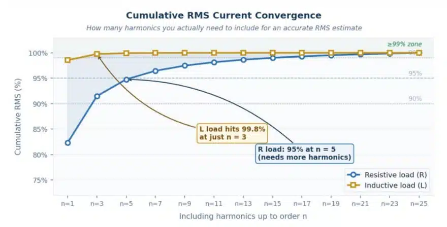
A truncated RMS estimate, using harmonics up to N based on this bandwidth, is usually sufficient and can be validated with SPICE FFT analysis. For inductive paths, contributions from high-order harmonics converge very quickly, while capacitive paths require careful consideration of the frequency range up to the capacitor’s self-resonant region.
Harmonic contributions: resistive vs inductive paths
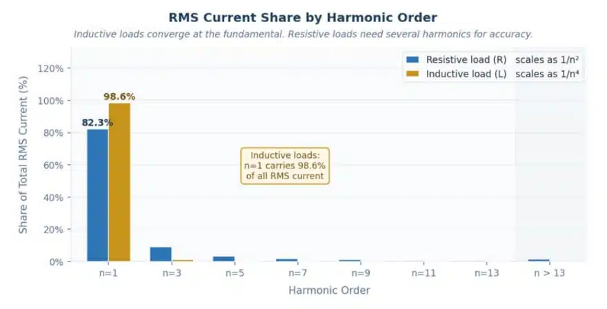
The distribution of RMS current over harmonics depends strongly on whether the path is mainly resistive or inductive. For a symmetrical square wave across a resistive path, current harmonics decay proportionally to 1/n, so higher harmonics accumulate more slowly but still contribute a meaningful share of total RMS current.
For an inductive path with , harmonic currents drop faster with order and the RMS contribution is dominated by the fundamental, often accounting for more than 98.5% of total RMS current, with the third harmonic pushing cumulative RMS above 99.7%. This explains why the inductor waveforms can often be approximated by fundamental plus low-order ripple when sizing copper and estimating losses.
Capacitor ripple at switching nodes: bandwidth and SRF
In capacitor ripple-current analysis at switching nodes, the situation is inverted: because capacitive impedance falls with frequency up to the self-resonant frequency (SRF), higher-order harmonics may dominate RMS current in idealized models. Real converters limit this via finite edge times and parasitic inductance, setting an effective upper bound to the relevant harmonic band.
MLCC and DC-link capacitor SRF, ESR/ESL, stack-up, and layout determine real-world current distribution and heating. Accurate estimation requires aligning harmonic analysis with these device- and layout-level characteristics, rather than stopping at the nominal switching frequency.
Practical tips for MLCCs at switching nodes
- Prefer multiple smaller MLCCs in parallel rather than a single large part to spread high‑frequency ripple current and reduce self‑heating.
- Check impedance vs frequency and SRF, and ensure dominant harmonics from the SW node sit well below the MLCC’s self‑resonant peak where current is still well controlled.
- Derate both voltage and ripple‑current capability versus datasheet limits, especially at elevated ambient and with strong high‑frequency content from fast edges.
- Minimize ESL and ESR by using small case sizes, short traces, and tight loops between SW node, MLCCs, and ground to reduce ringing and localized heating.
- Combine analytical harmonic estimates with SPICE/FFT or scope measurements of SW‑node current and voltage to validate MLCC temperature rise under worst‑case operation.
If you’d like this rewritten as a Yoast “How‑to” block specifically for “How to estimate MLCC ripple current at the SW node”, I can translate these into step‑by‑step format next.
Design implications for Power Electronics
For hard-switched buck, boost, flyback, and SEPIC converters, square-wave SW-node voltages drive inductor and capacitor currents according to the harmonic principles above. Inductor copper design can focus on low-order harmonics, while capacitor ripple-current limits must account for high-order content up to the effective bandwidth.
For resonant LLC converters, the tank filters much of the harmonic content in the main power path, but gate-drive, clamp, and auxiliary networks still see square-wave-like signals with rich harmonic content. Here, harmonic analysis informs snubber dimensioning, gate-drive design, and EMI filter cutoff selection.
The harmonic behavior discussed above translates directly into concrete design decisions for common power electronics components and converter topologies, as summarized in Tables 1 and 2.
| Component | Square‑wave / harmonic risk | Key design actions (frequency‑domain view) |
|---|---|---|
| Inductors | Elevated RMS current from low‑order harmonics at switching nodes (buck, boost, flyback, SEPIC). Fundamental often >98.5% of RMS in inductive paths. | Size copper and core for harmonic RMS current, not just DC; include at least first few harmonics in loss estimates; verify temperature rise with realistic ripple current; optimize layout to reduce parasitics that leak high‑frequency content into the inductor loop. |
| MLCCs / output caps | High ripple current from high‑order harmonics and fast edges at switching node or gate-drive rails; stress dominated by high frequency rather than DC. | Use parallel MLCCs to share ripple current; derate voltage and ripple current vs datasheet; check SRF and impedance vs frequency; include harmonic current in thermal estimates; minimize ESL/ESR via layout and package choice. |
| Bulk / DC‑link capacitors | Significant RMS current from lower and mid‑order harmonics of line or DC bus ripple and switching-node coupling; heating and lifetime impacted. | Verify RMS ripple current rating using harmonic analysis; choose technology (electrolytic, film, MLCC) to handle dominant harmonics; ensure adequate cooling and margin vs lifetime at operating temperature. |
| MOSFETs (power stage) | Switching device stress from dv/dt and di/dt; harmonic content influences voltage overshoot, ringing, and EMI. | Control edge rate to balance switching loss vs EMI; use appropriate snubbers/clamps tuned to dominant ringing frequencies; check SOA and repetitive stress at worst‑case harmonic conditions; validate with scope/FFT. |
| MOSFET gate drivers | Peak current demand into capacitive gate load proportional to dv/dt; fast edges increase harmonic content and driver dissipation. | Verify driver peak current vs required gate charge and edge rate; provide low‑inductance gate loop; consider gate resistors/series damping; check driver thermal dissipation at target switching frequency. |
| Rectifiers / synchronous FETs | Exposed to square‑like voltage and current waveforms; reverse recovery and body‑diode behavior coupled to harmonic content. | Select devices with suitable reverse recovery or use synchronous rectification; minimize parasitic inductances in loops; evaluate losses at realistic harmonic current spectra, not just DC. |
| EMI input/output filters | Excited by harmonic spectrum of switching waveforms and layout‑induced ringing. | Place filter cutoff below key harmonics identified in Fourier/FFT analysis; avoid resonance near dominant harmonics; provide damping where needed; co‑design filter with layout and snubbers. |
| Snubbers / clamp networks | Absorb energy at specific high‑frequency components and ringing modes. | Dimension snubber impedance and power rating based on measured or simulated ringing frequencies and amplitudes; ensure components can handle repetitive high‑frequency pulses and RMS dissipation. |
| Converter type | Key square‑wave locations | Dominant harmonic concerns | Practical design implications |
|---|---|---|---|
| Buck | High‑dv/dt SW node, gate-drive signals, synchronous FET node. | Low‑order harmonics dominate inductor RMS; higher harmonics stress MLCCs at SW node, excite EMI filter. | Size inductor for harmonic RMS current; check MLCC ripple at SW node with bandwidth‑limited harmonic model; design EMI filter cutoff below dominant harmonics; validate with FFT of SW node. |
| Boost | SW node at MOSFET drain, diode/synchronous FET node, gate drive. | Similar to buck, but higher voltage stress and often higher dv/dt; harmonics strongly excite diode/synchronous rectifier transitions. | Include harmonic-induced RMS inductor current when sizing high‑voltage boost inductors; pay attention to diode reverse‑recovery stress at high di/dt; ensure EMI filter and snubbers handle dominant switching harmonics. |
| Flyback | Primary switch node, secondary rectifier, clamp/snubber network. | Square‑like primary and secondary waveforms with strong high‑frequency components during transitions; clamp networks see concentrated harmonic energy. | Size primary inductance and copper for harmonic RMS current; design RCD/active clamps based on energy at ringing frequencies; verify rectifier current spectrum vs ratings; include harmonic ripple in capacitor stress, especially on secondary. |
| SEPIC | Two inductors (or coupled inductor), multiple switching nodes, series coupling capacitor. | Multiple square‑wave nodes increase harmonic paths; coupling capacitor sees large high‑frequency ripple. | Evaluate harmonic RMS currents in both inductors and coupling capacitor; select MLCCs/film caps for high ripple and SRF; pay attention to EMI filter design due to extra nodes; validate via FFT of both switching nodes. |
| LLC resonant | Half‑bridge/full‑bridge drive, resonant tank, rectifier. | Tank filters much of the high‑frequency content in the power path, but square‑like drive and gate waveforms still contain harmonics; off‑resonance operation changes spectral distribution. | Use harmonic analysis mainly for gate-drive, clamp, and EMI structures; confirm that tank components are sized for near‑sinusoidal currents; evaluate rectifier and output caps under the resulting current spectrum rather than ideal sine assumptions. |
| DAB / phase‑shifted full bridge | Bridge legs generate square‑wave voltages; transformer primary/secondary see phase‑shifted square waves modulated at switching frequency. | Harmonic content depends on phase shift; certain harmonics can be reinforced or cancelled; transformer and leakage inductance define effective bandwidth. | Analyze bridge output using harmonic decomposition for key phase‑shift cases; size transformer copper/core for RMS currents including harmonics; verify that leakage and snubbers manage high‑frequency components; consider EMI impact of phase‑shift modulation. |
Summary
Square-wave voltages are fundamental to power converter operation and cannot be accurately analyzed using only DC or single-frequency sinusoidal methods. Harmonic decomposition provides a rigorous yet practical framework for calculating currents in inductors, capacitors, and switching devices, improving the fidelity of loss, thermal, and reliability predictions across buck, boost, flyback, SEPIC, and LLC/DAB designs.
Source
This article is expanded and adapted from the original source application note “Calculating Current Induced by Square-Wave Voltages in Power Electronics Circuits” by Jake Michels, YAGEO Group.
Further Reading
For readers wanting deeper topology-specific context, see:
- Buck converter design and calculation
- Boost converter design and calculation
- Flyback converter design and calculation
- SEPIC converter design and calculation
- LLC resonant converter design and calculation
- Power converter dossier
FAQ: RMS Square Harmonics in Power Converters
Square‑wave harmonics are the sinusoidal frequency components that make up a square‑wave switching waveform in power converters. They occur at odd multiples of the switching frequency and significantly influence RMS currents, electromagnetic interference, and component stress.
Inductors have impedance that increases with frequency, so higher‑order harmonic currents drop quickly with harmonic order. In typical inductive paths, more than 98.5% of RMS current is carried by the fundamental and only a few low‑order harmonics, which is critical for accurate copper‑loss and thermal design.
Capacitors have impedance that decreases with frequency up to their self‑resonant region, so higher‑order harmonics can drive large ripple currents through MLCCs and DC‑link capacitors. This increases self‑heating and can limit lifetime even when DC voltage and low‑frequency ripple look modest.
First decompose the square‑wave voltage into its harmonic components using the Fourier series. Then evaluate the circuit impedance at each harmonic, compute the harmonic currents, and combine them using RMS summation up to a harmonic order that matches the effective bandwidth of the converter and components.
Gate‑driver current is largely set by charging and discharging the MOSFET gate capacitance with a square‑wave voltage. Fast edges add high‑frequency harmonics that increase peak driver current and dissipation, so harmonic‑based estimates help verify driver current capability, loop layout, and gate‑resistor selection.
Hard‑switched buck, boost, flyback, and SEPIC converters are strongly affected because their switching nodes and rectifiers see square‑like voltages. Resonant LLC and phase‑shifted full‑bridge or DAB converters also generate rich harmonic content at gate‑drive, clamp, transformer, and EMI‑filter nodes that must be considered in design.
EMI filters are driven by the harmonic spectrum of switching waveforms and layout‑induced ringing. Knowing which harmonics dominate allows you to place filter cutoff frequencies, damping networks, and snubbers so they effectively attenuate those components without creating unwanted resonances.
How to estimate RMS currents from square‑wave voltages in a power converter
- Step 1 – Identify the relevant square‑wave node
Choose the switching node, gate‑drive node, or clamp/rectifier node whose current you want to analyze, such as the SW node of a buck converter inductor or the gate of a power MOSFET.
- Step 2 – Define the square‑wave parameters
Determine the peak or peak‑to‑peak voltage, switching frequency, and duty cycle of the waveform under your worst‑case operating condition. These parameters are the basis for the Fourier series representation.
- Step 3 – Decompose the waveform into harmonics
Use the Fourier series of a symmetric square wave to calculate the amplitude of each harmonic of the voltage. For a simple case, only odd harmonics are present and the nth harmonic amplitude decreases approximately as 1/n.
- Step 4 – Determine circuit impedance at each harmonic
For the current path of interest, compute the impedance at each harmonic frequency, including parasitics where relevant. For example, use Z_L = jωL for an inductor, Z_C = 1/(jωC) for a capacitor, or the full impedance of an EMI filter branch.
- Step 5 – Calculate harmonic current amplitudes
For each harmonic, divide the harmonic voltage amplitude by the corresponding impedance magnitude to obtain the harmonic current. Repeat for all harmonics up to the limit set by rise/fall times and component self‑resonant frequencies.
- Step 6 – Compute total RMS current
Combine the harmonic currents using RMS summation by squaring each harmonic current, summing the squares, and taking the square root. This gives an accurate estimate of RMS current that includes both fundamental and harmonic contributions.
- Step 7 – Apply results to component sizing and verification
Use the calculated RMS current to verify current ratings, loss and thermal margins for inductors, capacitors, gate drivers, rectifiers, snubbers, and EMI filters. Adjust component selection, layout, or edge‑rate control as needed to keep temperatures, ripple, and EMI within specification.